Avoiding Component Misalignment in PCB Assembly
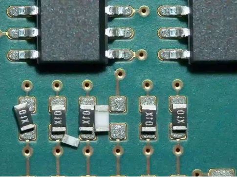
Table of Contents
In the intricate world of electronics manufacturing, the precise placement of every single component on a Printed Circuit Board(PCB) is paramount. The slightest deviation, known as component misalignment, can compromise the entire functionality and reliability of an electronic device. As circuits become more complex and components shrink, the challenges associated with achieving and maintaining perfect alignment in PCB assembly processing are amplified. This article delves into the critical aspects of component misalignment, exploring its causes, the profound impact it has on product performance, and the robust strategies employed for its detection and prevention, particularly within the context of modern SMT assembly.
1. Understanding Component Misalignment
Component misalignment refers to any deviation of a component from its intended position on the PCB pad during the assembly process. This can range from a minor shift, where a component is slightly off-center but still makes electrical contact, to severe displacement leading to bridging, open circuits, or complete detachment. Misalignment manifests in various forms:
- Lateral Shift:The component is shifted horizontally or vertically from its ideal center.
- Rotational Misalignment:The component is rotated on its axis relative to the pad.
- Tombstoning:A common issue where one end of a chip component lifts off the pad during reflow, resembling a tombstone. This is often caused by unbalanced surface tension forces on the solder joints.
- Bridging:Solder connecting two adjacent pads that should be isolated, often due to a component shifting too close.
- Floating:A component that has completely detached or is barely connected, creating an open circuit.
Even a microscopic shift can have significant consequences, especially with fine-pitch components and BGA packages where pad sizes are extremely small. Maintaining precise alignment is a cornerstone of quality in manufacturing.
2. The Critical Impact on PCB Reliability
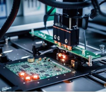
The ramifications of component misalignment extend far beyond aesthetic imperfections. It directly impacts the electrical integrity and long-term reliability of the Printed Circuit Board, leading to a cascade of potential issues:
1) Electrical Malfunctions:
- Open Circuits:Misaligned components may fail to make proper electrical contact with one or more pads, leading to open circuits and non-functional connections.
- Short Circuits:Components shifted too close to adjacent pads can create unintended electrical bridges, causing short circuits, current leakage, and potential device failure.
- Intermittent Connections:Slight misalignments might result in unreliable contacts that work inconsistently, making troubleshooting exceedingly difficult.
2) Reduced Product Lifespan: Stress on misaligned solder joints can lead to premature fatigue and failure, shortening the operational life of the electronic device.
3) Costly Rework and Scrap: Identifying and rectifying misaligned components often requires intricate rework, which is time-consuming and expensive. In severe cases, entire boards may need to be scrapped, leading to significant material and labor losses.
4) Field Failures and Reputation Damage: Products with latent misalignment defects can fail in the field, leading to warranty claims, product recalls, and severe damage to a brand’s reputation and customer trust.
5) Performance Degradation: Even if not catastrophic, misalignment can alter electrical characteristics, impacting signal integrity, power delivery, and overall device performance, especially in high-frequency applications.
Given these profound consequences, preventing misalignment is not just a quality control measure; it’s a fundamental requirement for producing reliable, high-performance electronics.
3. Root Causes of Component Misalignment in SMT Assembly
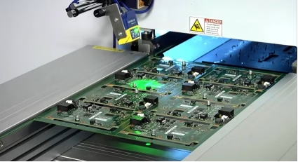
Achieving perfect alignment in SMT assembly is a complex endeavor, with numerous factors contributing to potential component misalignment. Understanding these root causes is crucial for effective prevention.
3.1 Stencil Printing Issues
The solder paste printing process is the first critical step and a major source of misalignment issues.
- Incorrect Stencil Aperture Design:Improperly sized or shaped apertures can lead to too much or too little solder paste deposition, affecting component wetting and placement.
- Squeegee Pressure and Speed:Inconsistent pressure or speed can cause uneven paste deposition, leading to potential shifts during reflow.
- Worn Stencils:Damaged or worn stencils can result in blurry or inconsistent paste prints.
- Poor Board Support:Inadequate support for the PCB during printing can cause bowing, leading to uneven paste application.
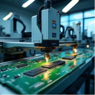
3.2 Pick-and-Place Machine Accuracy
The precision of the pick-and-place machine is paramount.
- Worn Nozzles:Damaged or clogged nozzles can fail to pick up components correctly or place them with insufficient force/vacuum, leading to detachment or misalignment.
- Calibration Errors:Miscalibrated machine vision systems or placement heads can cause consistent offset errors.
- Component Recognition Issues:The vision system failing to accurately identify component fiducials or body outlines can lead to incorrect orientation or placement.
- Vibration:Machine vibration or instability can cause components to shift during transfer.
3.3 Solder Paste Characteristics
The properties of the solder paste itself play a significant role.
- Viscosity:Incorrect paste viscosity can lead to slumping(spread) or insufficient tackiness, making components prone to movement.
- Slump:If the solder paste slumps after printing, it can bridge between pads before components are even placed, or after, increasing the risk of shorts.
- Tackiness:Insufficient tackiness means components won’t be held securely in place before reflow.
- Oxidation:Oxidized solder paste can hinder proper wetting and create inconsistent surface tension.
3.4 Component Packaging and Handling
The quality of components and how they are handled before placement can also contribute to issues.
- Component Warpage:Bent or warped components are difficult to place accurately and may lift during reflow.
- Inconsistent Packaging:Poorly taped components in feeders can lead to improper pick-up by the machine.
- Moisture Sensitivity :Moisture-sensitive components can delaminate or popcorning during reflow, affecting alignment.
3.5 Reflow Soldering Profile
The reflow oven profile is critical for proper solder joint formation and can induce or rectify misalignment.
- Rapid Heating/Cooling:Too rapid heating or cooling can cause thermal shock, leading to component movement or stress.
- Insufficient Preheat:If the preheat zone is too short, the solvent in the paste may not fully evaporate, leading to outgassing and component movement during reflow.
- Temperature Gradients:Uneven temperatures across the PCB can cause differing surface tension forces, particularly leading to tombstoning.
- Insufficient Dwell Time in Reflow:Not enough time at peak temperature can result in poor wetting and weak joints susceptible to movement.
3.6 Board Design and Quality
Issues inherent in the PCB design or manufacturing can also play a role.
- Pad Design:Unevenly sized pads or incorrect pad-to-component ratios can lead to imbalanced surface tension during reflow.
- Board Flatness:Warped PCBs can lead to inconsistent paste printing and component placement.
- Surface Finish:Inconsistent or poor surface finishes can affect solder wetting and adhesion.
4. Advanced Detection and Inspection Methods

Detecting component misalignment early and effectively is crucial to prevent defective products from reaching the market. Modern PCB assembly lines employ sophisticated inspection technologies:
1) Automated Optical Inspection(AOI):
- AOI systems use high-resolution cameras and advanced algorithms to visually inspect PCBs for defects immediately after solder paste printing, component placement, and reflow. They can quickly identify shifts, rotations, missing components, incorrect polarity, and other visual anomalies.
- Post-reflow AOI is particularly effective at catching tombstoning, bridging, and lateral shifts that become apparent after soldering.
2) Automated X-ray Inspection(AXI):
- For packages where solder joints are hidden beneath the component(e.g., BGAs, QFNs), AXI is indispensable. It uses X-rays to create images of the solder joints, allowing inspection for voids, shorts , and precise alignment, even for hidden connections.
- 2D and 3D AXI systems can provide detailed insights into solder joint quality and component position that are invisible to optical systems.
3) Solder Paste Inspection(SPI):
- SPI systems are deployed immediately after solder paste printing to verify the volume, height, shape, and alignment of the deposited paste. Since 70-80% of all soldering defects originate from printing, SPI is a critical proactive detection tool.
- By detecting paste misalignment or insufficient volume, it prevents issues before components are even placed.
4) Manual Inspection: While largely replaced by automated systems for high-volume production, manual inspection using microscopes is still used for complex boards, prototyping, or specific troubleshooting, particularly for larger components or visually obvious defects.
The combination of these technologies forms a robust quality control framework, allowing manufacturers to catch and address misalignment issues at various stages of the PCB assembly process.
5. Strategies for Prevention and Mitigation
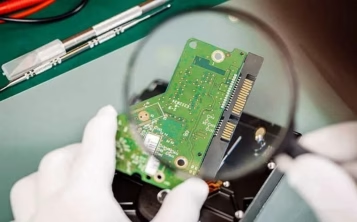
Proactive measures are far more effective and cost-efficient than reactive defect detection. A multi-faceted approach is required to minimize component misalignment:
5.1 Design for Manufacturability(DFM)
Integrating manufacturability considerations early in the design phase can significantly reduce misalignment risks.
- Optimized Pad Geometries:Designing appropriate pad sizes and shapes for each component, considering solder mask defined(SMD) vs. non-solder mask defined(NSMD) pads, can promote even solder wetting and prevent tombstoning.
- Component Spacing:Adequate spacing between components and pads helps prevent bridging and provides tolerance for minor shifts.
- Fiducial Marks:Incorporating global and local fiducial marks on the PCB allows placement machines to precisely align the board and components.
5.2 Process Optimization and Control
Meticulous control over the SMT assembly process parameters is vital.
- Solder Paste Management:Ensure correct solder paste type, proper storage(temperature, humidity), and timely replacement. Monitor paste viscosity and print quality regularly.
- Reflow Profile Optimization:Develop and fine-tune reflow profiles specific to the board and component mix. Ensure proper preheat, soak, reflow, and cooling zones to minimize thermal stress and maximize self-alignment.
- Placement Parameters:Optimize pick-and-place force, speed, and vacuum settings for each component type.
5.3 Equipment Maintenance and Calibration
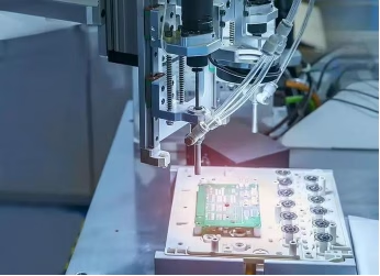
Regular maintenance and calibration of all assembly equipment are non-negotiable.
- Pick-and-Place Machine Maintenance:Regular cleaning and replacement of worn nozzles, verification of vision system calibration, and routine preventative maintenance are crucial for placement accuracy.
- Printer Maintenance:Keep stencil printers clean, ensure proper squeegee condition, and verify print alignment.
- Oven Maintenance:Ensure reflow ovens maintain consistent temperature profiles across all zones and channels.
5.4 Material Quality Control
Inspecting incoming materials ensures they meet specifications.
- Component Quality:Source high-quality components that are free from warpage, damage, or manufacturing defects.
- PCB Quality:Verify board flatness, pad integrity, and surface finish.
- Solder Paste Quality:Use reputable brands and ensure proper storage and handling to prevent degradation .
5.5 Operator Training and Experience
Well-trained operators are less likely to make errors that lead to misalignment.
- Machine Operation:Ensure operators are proficient in setting up and operating SMT equipment.
- Troubleshooting:Train staff to identify common issues and implement immediate corrective actions.
- Handling Procedures:Proper handling of PCBs and components minimizes physical damage or contamination.
By implementing these comprehensive strategies, manufacturers can significantly reduce the incidence of component misalignment, enhancing product quality and reducing production costs.
6. The Future of Precision PCB Assembly
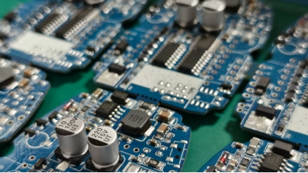
The drive for miniaturization and increased functionality continues to push the boundaries of PCB assembly precision. Future advancements will likely focus on even greater automation, data-driven process control, and predictive maintenance:
- Smart Factory Integration:Leveraging IoT sensors and AI to monitor every stage of the assembly line in real-time, providing immediate feedback and predictive analytics to prevent misalignment before it occurs.
- Advanced Vision Systems:Next-generation vision systems with higher resolution, faster processing, and machine learning capabilities will offer unparalleled accuracy in component placement and defect detection.
- Robotics and Cobots:Collaborative robots will increasingly assist in component handling and intricate assembly tasks, further reducing human error.
- Additive Manufacturing:Emerging technologies like 3D printing for electronic components or even entire PCBs may offer new ways to embed components directly, potentially eliminating traditional misalignment challenges.
The pursuit of zero-defect manufacturing in Printed Circuit Board production is an ongoing journey, with technology continually evolving to meet the demands of an increasingly complex electronic landscape.
7. Component Misalignment FAQs
Question1: What is the most common type of component misalignment?
Lateral shift and tombstoning are among the most frequently observed types of component misalignment, especially for smaller chip components during the reflow process.
Question2: How much misalignment is acceptable in PCB assembly?
Acceptable misalignment tolerances depend heavily on component package type, pitch, and application. For fine-pitch components(e.g., BGA), even a few tens of micrometers can be critical. Industry standards(like IPC) provide guidelines, but typically, misalignment should be within 25-50% of the pad width to ensure reliable solder joint formation.
Question3: Can component misalignment be repaired?
Yes, minor misalignments can often be repaired through rework processes using specialized tools like hot air rework stations and microscopes. However, extensive misalignment or damage may require scrapping the board, and rework is always more costly and time-consuming than prevention.
Question4: What role does solder paste play in preventing misalignment?
Solder paste is critical. Its correct volume, tackiness, and viscosity ensure that components are held securely after placement and self-align properly during reflow due to surface tension, minimizing misalignment. Improper paste can lead to shifting, tombstoning, or bridging.
Question5: Is manual inspection still relevant for detecting misalignment?
While automated optical inspection(AOI) and X-ray inspection(AXI) are the primary methods for high-volume production, manual inspection still has its place for verifying complex components, low-volume prototypes, or investigating specific failure modes that automated systems might flag. However, it is prone to human error and fatigue.
8. Summary
Component misalignment in PCB assembly processing is a pervasive and critical challenge that directly impacts the reliability and performance of electronic devices. From subtle lateral shifts to severe tombstoning, these defects arise from a multitude of factors across the manufacturing chain, including issues with solder paste printing, pick-and-place machine accuracy, component handling, and reflow soldering profiles. The consequences range from immediate electrical failures to long-term product degradation and costly rework.
Effective mitigation relies on a combination of advanced detection technologies like AOI, SPI, and AXI, alongside robust preventive strategies. These strategies encompass meticulous design for manufacturability(DFM), stringent process control, regular equipment maintenance, stringent material quality checks, and comprehensive operator training. As SMT assembly continues to evolve with smaller, denser components, the pursuit of precision remains paramount, driving innovations towards smarter, more automated, and predictive manufacturing environments to achieve near-zero defects.
Contact us
WhatsApp: +86-13570802455
Wechat: +86-13570802455
Email: [email protected]