Thick Copper PCB
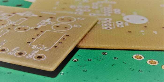
Table of Contents
Y&T TECHNOLOGY · MANUFACTURING SERVICES
Heavy-copper PCB fabrication
Use the technical information below to prepare a project-specific quotation.
- Specify finished copper per layer, current-carrying geometry, stack-up, thermal requirements and finish.
- Include quantity, approved drawing revision, inspection requirements and target delivery date.
Quote heavy copper with the full construction
Send with your request
- Specify finished copper weight for each layer and the complete stack-up.
- Provide trace spacing, high-current regions, thermal paths and finished board thickness.
- Identify plated holes, solder mask clearances and critical flatness requirements.
Agree before the order starts
- Review copper thickness and local feature dimensions together.
- Confirm thermal, dimensional and electrical acceptance requirements before release.
Include quantity, delivery destination and requested date. Your quotation identifies the accepted scope, exceptions, documentation and schedule.
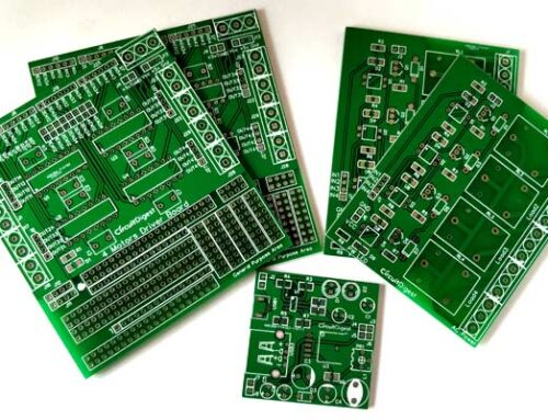
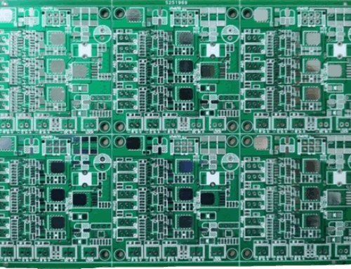
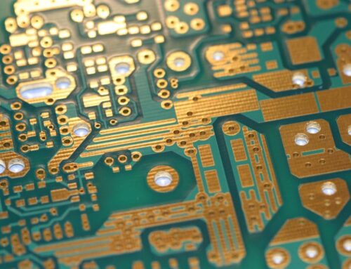
Thick copper PCB products are used extensively in power electronic devices and power supply systems. A growing trend in the PCB industry, this unique type of heavy copper PCB features a finished copper weight of more than 4oz (140μm), compared to the 1oz (35μm) or 2oz (70μm) copper weight generally found in those with a standard PCB copper thickness.
The additional copper PCB thickness enables the board to conduct a higher current, achieve good thermal distribution and implement complex switches in a limited space. Other advantages include increased mechanical strength at connector sites, the ability to create a smaller product size by incorporating multiple weights on the same layer of circuitry and the ability to use exotic materials to their maximum capacity with minimal risk of circuit failure.
Copper PCB Manufacturing Capabilities Table
Y&T Technology is a highly skilled PCB manufacturer that can develop and produce a superior thick copper PCB product of the highest quality. We offer a thick copper PCB manufacturing service that reviews the required copper weight, units and stack-up for the specific design. Check our capabilities in the following table:
| Feature | Information for engineering review |
| Quality Grade | Required IPC standard, revision, acceptance class and inspection scope agreed in the quotation. |
| Number of Layers | Provide the layer count and complete stack-up; engineering confirms the accepted construction. |
| Order Quantity | Provide initial and repeat-order quantities. Accepted batch size, panel utilization and charges are confirmed per project. |
| Build Time | Fabrication lead time and any accepted rush option are confirmed after material, construction, quantity and production review. This is separate from assembly and international transit. |
| Material | Specify the manufacturer, grade, datasheet revision and required material declarations; availability and substitutions require confirmation. |
| Board Size | Supply finished outline and panel drawing with units and dimensional tolerances; accepted dimensions are confirmed by engineering. |
| Board Thickness | Specify the finished thickness, stack-up and tolerance. Engineering confirms the achievable combination for your construction. |
| Max Outer Layer Copper Weight (Finished) | Specify starting and finished copper, units, layer location and tolerance. Feasibility is confirmed with the stack-up. |
| Max Inner Layer Copper Weight | Specify starting and finished copper, units, layer location and tolerance. Feasibility is confirmed with the stack-up. |
| Min Tracing/Spacing | Provide trace and spacing requirements with units, copper weight and layer location; engineering confirms the design limits. |
| Solder Mask Sides | Specify mask sides, colour, openings, registration and any special acceptance requirements for review. |
| Solder Mask Color | Specify mask sides, colour, openings, registration and any special acceptance requirements for review. |
| Silkscreen Sides | Specify legend sides, colour, minimum text and registration requirements in the fabrication data. |
| Silkscreen Color | Specify legend sides, colour, minimum text and registration requirements in the fabrication data. |
| Surface Finish | Specify the finish or plating system, applicable standard, thickness and documentation required for the project. |
| Min Annular Ring | Identify drilled versus finished PTH or NPTH dimensions, units, tolerances and applicable stack-up for engineering review. |
| Min Drilling Hole Diameter | Identify drilled versus finished PTH or NPTH dimensions, units, tolerances and applicable stack-up for engineering review. |
| Other Techniques | Identify the required special process, via construction, edge treatment or inspection. Engineering confirms availability and any tooling or cost impact. |
Finished Copper PCBs of Superior Quality
Y&T Technology has a decade of experience in manufacturing and assembling high-performing standard and heavy copper PCB products that help our customers achieve their productivity and profitability goals. We make it a standard operating procedure to have our highly skilled engineers run design for manufacture on every circuit file, and address all questions and concerns before production. This helps to ensure the finished electronic boards meet your performance expectations. Our capable staff includes an in-house quality control department – inspection scope and acceptance criteria are agreed for the quoted project.
(Note: To ensure we can fabricate your thick copper PCB correctly, it is important to take the greater width of traces and spacing between the traces caused by the increased copper weight into consideration.)
Get Custom Quotation for Your Thick Copper PCB Project
Please click below button to enter our PCB Quote page, then fill in your circuit spec and submit;We will reply you as soon as possible by Email.
Quote for Thick Copper PCB Fabrication
If you got questions about our Thick Copper PCB manufacturing capabilities or your custom project required specifications are not listed in this page,Please feel free to contact us. Quote timing is confirmed after file and material review.
Contact us
WhatsApp: +86-13570802455
Wechat: +86-13570802455
Email: [email protected]