What are PCB Guard Ring? How to avoid common layout errors?
Table of Contents
In the intricate world of Printed Circuit Board (PCB) design, achieving optimal signal integrity and precision, especially in analog and mixed-signal circuits, presents numerous challenges. Among these, managing leakage currents and mitigating noise are paramount. This is where the often-underestimated but critically important concept of a PCB guard ring comes into play. Guard rings are specialized conductive traces designed to protect sensitive circuit nodes from unwanted leakage currents and environmental noise, ensuring the reliability and accuracy of high-impedance and low-current applications.
This comprehensive guide delves into the fundamental principles, design considerations, and practical applications of PCB guard rings, offering engineers and designers the knowledge to implement them effectively in their projects.
1. What is a PCB Guard Ring?
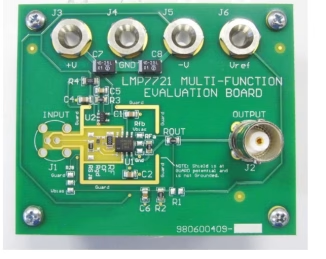
A PCB guard ring is essentially a conductive trace or ring that encircles a sensitive node or area on a PCB, designed to intercept and divert undesirable leakage currents away from the protected signal. These currents, often minute but significant in high-impedance circuits, can originate from various sources, including the PCB substrate itself (surface and bulk leakage), environmental contaminants, or parasitic paths formed by adjacent traces.
The primary mechanism by which a guard ring operates is by providing a low-impedance path for these leakage currents, effectively “guarding” the sensitive node. Instead of flowing into or out of the protected trace, the leakage current is shunted to a controlled potential, typically ground or a potential very close to the guarded signal. This action dramatically reduces errors and maintains the integrity of the critical signal path.
2. Why PCB Guard Rings Are Crucial: Benefits and Applications
The strategic implementation of guard rings yields several significant benefits, particularly in circuits demanding high precision and low noise:
- Preventing Leakage Current:This is the most critical function. In high-impedance circuits (e.g., those with input impedances in the giga-ohms or tera-ohms), even picoamperes of leakage current can cause substantial voltage errors across large resistances. Guard rings divert these currents, preserving signal accuracy.
- Improving Signal Integrity:By isolating sensitive traces, guard rings help prevent crosstalk and coupling from noisy adjacent signals, ensuring the integrity of the desired signal.
- Reducing Measurement Errors:In applications like sensor interfaces (e.g., pH sensors, photodiodes), electrometer circuits, or high-precision Analog-to-Digital Converters (ADCs), guard rings are indispensable for achieving stable and accurate measurements.
- Shielding and Noise Reduction:A guard ring can act as a shield, protecting sensitive traces from external electromagnetic interference (EMI) and internal noise sources present on the PCB.
- EnhancingCircuit Stability: By minimizing uncontrolled current paths, guard rings contribute to the overall stability and predictability of circuit behavior, especially in temperature-sensitive designs.
- ESD Protection (Secondary Benefit):While not their primary role, a properly grounded guard ring around a sensitive input can offer some degree of ESD protection by providing a low-impedance path for transient discharge.
Common applications where guard rings are essential include medical instrumentation, precision test and measurement equipment, scientific research apparatus, and any system dealing with very low currents or high input impedances.
3. Types of PCB Guard Rings and Their Use Cases
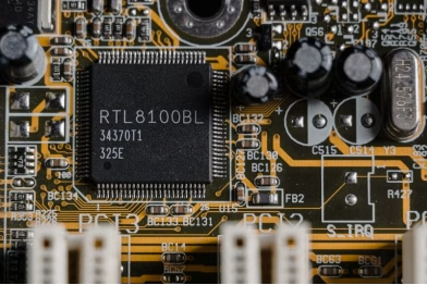
Guard rings can be broadly categorized based on the potential they are connected to, each serving slightly different purposes:
3.1 Driven Guard Rings (Active Guard Rings)
A driven guard ring is connected to a potential that is equal to, or very nearly equal to, the potential of the sensitive trace it is guarding. This is typically achieved by connecting the guard ring to the output of a buffer amplifier that mirrors the input signal. This type is particularly effective for high-impedance input nodes, such as the non-inverting input of an operational amplifier. By maintaining the guard ring at the same potential as the input, there is virtually no voltage difference across the insulation between the guarded trace and the guard ring, thus eliminating any leakage current across that interface.
Use Cases:
- Op-amp input pins (e.g., inverting or non-inverting inputs).
- High-impedance sensor outputs (e.g., photodiode current-to-voltage converters).
- Electrometer circuits.
3.2 Ground Guard Rings (Passive Guard Rings / PCB Ground Ring / Guard Trace)
A ground guard ring, also referred to as a PCB ground ring or simply a guard trace when it’s a single trace, is connected directly to the circuit’s ground plane. This is the most common and often easiest type of guard ring to implement. Its primary function is to provide a low-impedance path to ground for leakage currents originating from areas surrounding the sensitive trace or to shield a sensitive trace from noisy digital signals.
Use Cases:
- Isolating sensitive analog traces from noisy digital lines.
- Surrounding sensitive components to divert substrate leakage.
- Acting as a return path for shields or other ground connections.
- Separating analog and digital ground planes (though a full split plane is often preferred).
3.3 Analog/Digital Isolation Guard Rings
While often a form of ground guard ring, this specific application focuses on creating clear boundaries between sensitive analog circuitry and noisy digital sections. A guard ring (connected to analog ground) can encircle analog components to prevent digital switching noise from coupling into the analog domain, effectively creating a “quiet zone” on the PCB.
4. PCB Guard Ring Layout and Routing Best Practices

Effective implementation of a guard ring layout requires careful consideration during the PCB design phase. Here are key best practices for guard ring routing:
1) Placement: The guard ring must completely encircle the sensitive node or trace. For op-amp inputs, it should encircle the input pad and extend around the trace leading to it, preferably on the top layer where the component is mounted.
2) Proximity: The guard ring should be placed as close as possible to the guarded trace without touching it. A typical spacing might be 0.1 mm to 0.3 mm (4 to 12 mils). This minimizes the resistance of the leakage path to the guard ring and reduces parasitic capacitance between the guarded trace and other noisy elements.
3) Width: The width of the guard ring trace itself should be sufficient for manufacturing and to ensure a robust low-impedance path. A width of 0.25 mm to 0.5 mm (10 to 20 mils) is often adequate.
4) Continuous Ring: Ensure the guard ring is a continuous, unbroken loop. Any break compromises its effectiveness by creating new leakage paths.
5) Connection Point (for Driven Guard Rings): For driven guard rings, connect the guard trace directly to the output of the buffer amplifier that mirrors the sensitive input. This connection should be short and direct.
6) Connection Point (for Ground Guard Rings): Ground guard rings should be connected to a clean ground reference, preferably via multiple vias to a solid ground plane to ensure a low-impedance path to ground. Avoid connecting it to a noisy ground return path.
7) Solder Mask Clearance: Ensure there is sufficient solder mask clearance around the guard ring. This prevents stray conductive materials (like solder paste or flux residue) from bridging the gap between the guarded trace and the guard ring, or between the guard ring and other traces.
8) Layer Considerations: Ideally, the guard ring should be on the same layer as the sensitive trace it is protecting. For multi-layer boards, consider extending the guard ring on adjacent layers (if practical) or placing a ground plane beneath the guarded area to further enhance shielding.
9) No Traces Crossing: Absolutely no other traces should cross the gap between the guarded trace and the guard ring. This creates parasitic capacitance and undermines the guard ring’s purpose.
10) Humidity and Contamination: While not strictly a layout rule, remember that surface leakage can be significantly exacerbated by humidity and contamination. Guard rings help, but proper board cleaning and conformal coating are additional measures for extreme environments.
Here’s a comparison of key aspects:
| Feature | Driven Guard Ring | Ground Guard Ring |
| Connection Potential | Potential equal to guarded trace (e.g., buffer output) | System ground (GND) |
| Primary Purpose | Eliminate leakage current across insulation | Divert leakage current to ground, provide shielding |
| Complexity | Requires active buffer, more complex routing | Simpler to implement, just connect to ground |
| Effectiveness | Highly effective for high-impedance inputs | Effective for general isolation and shielding |
| Typical Use | Op-amp inputs, electrometer circuits | Around sensitive analog sections, between analog/digital |
5. Common Pitfalls to Avoid
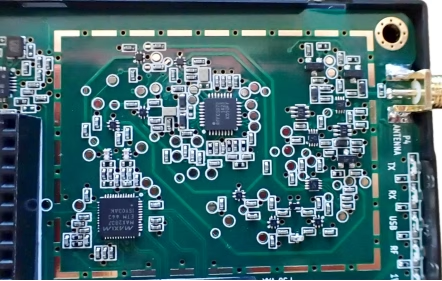
Even with good intentions, designers can make mistakes that diminish the effectiveness of guard rings:
- Breaking the Ring:Any discontinuity in the guard ring, even a small gap, compromises its ability to fully intercept leakage currents.
- Improper Connection:Connecting a driven guard ring to the wrong potential (e.g., ground instead of the buffer output) or a ground guard ring to a noisy ground can make matters worse.
- Too Far Apart :If the guard ring is too far from the sensitive trace, it might not effectively capture all leakage currents, or it could introduce unwanted parasitic capacitance with other signals.
- Traces Crossing the Gap:Allowing other signal traces to pass between the guarded trace and the guard ring creates new leakage paths and parasitic coupling, defeating the purpose.
- Ignoring Substrate Leakage:While guard rings address surface leakage, remember that bulk leakage through the PCB substrate can also be a factor, especially with very high impedance circuits. Material selection can help.
6. PCB Guard Ring FAQs
A ground plane provides a large, low-impedance return path for currents and general shielding. A guard ring is a specialized trace specifically designed to intercept and divert leakage currents from a particular sensitive trace by surrounding it with a potential either equal to the guarded trace (driven) or ground (passive).
Guard rings are essential in circuits dealing with extremely high input impedances (above 1 MΩ), very low currents (nanoamperes or picoamperes), or those requiring high precision and stability where even tiny leakage currents can introduce significant errors, such as in sensor interfaces, electrometers, or precision ADCs.
While guard rings primarily combat leakage currents and offer some shielding against localized electric field coupling, they are not a complete solution for all noise issues. They are less effective against magnetic field interference or common-mode noise without additional design techniques.
Typically, the most critical guard ring is on the top layer, directly adjacent to the sensitive component and trace. For enhanced shielding, a ground plane immediately below the guarded trace (on an inner layer) is beneficial. Extending guard rings to multiple layers can add complexity and is often only necessary in extremely sensitive, high-frequency, or high-impedance designs.
The main purpose is to shield sensitive traces and components from unwanted electromagnetic interference (EMI), crosstalk, and leakage currents, thereby improving signal integrity and circuit stability.
Not always. While connecting to a stable ground plane is common for EMI shielding and diverting some leakage, for high-impedance inputs, the guard ring might be connected to a low-impedance buffer output that follows the sensitive node’s potential. This helps prevent leakage current from flowing into the sensitive node.
7. Summary
PCB guard rings are a powerful tool in the arsenal of an electronics designer, indispensable for crafting high-performance analog and mixed-signal circuits. By understanding their purpose–to provide a controlled path for leakage currents and offer localized shielding-engineers can significantly enhance the accuracy, stability, and reliability of their designs. From preventing minute substrate leakage to isolating sensitive signals, careful implementation of guard rings is a hallmark of professional PCB design.
Key Takeaways
- Purpose:Guard rings intercept and divert unwanted leakage currents from sensitive PCB traces.
- Types:Driven guard rings (connected to a potential equal to the guarded trace) are for high-impedance inputs; Ground guard rings (connected to ground) are for general isolation and shielding.
- Benefits:Improve signal integrity, reduce measurement errors, enhance accuracy, and offer localized shielding.
- Layout Rules:Must be continuous, close to the guarded trace, appropriately wide, and connected to the correct potential. No traces should cross the guarded-trace-to-guard-ring gap.
- Applications:Critical for high-precision analog, sensor interfaces, and low-current applications.
Contact us
WhatsApp: +86-13570802455
Wechat: +86-13570802455
Email: [email protected]