High Frequency PCB
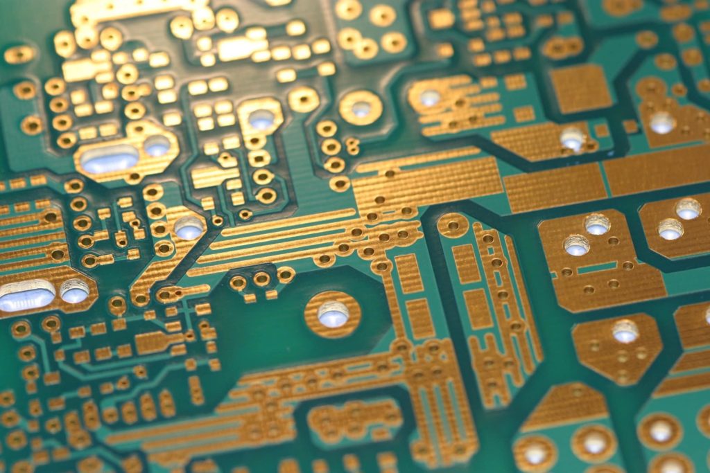
Table of Contents
Y&T TECHNOLOGY · MANUFACTURING SERVICES
RF and high-frequency PCB fabrication
Use the technical information below to prepare a project-specific quotation.
- Identify the laminate grade, frequency range, impedance targets, stack-up and copper requirements.
- Include quantity, approved drawing revision, inspection requirements and target delivery date.
RF PCB material and impedance requirements
Send with your request
- Specify operating frequency, laminate grade and required stack-up.
- Provide controlled impedance values, tolerance and reference planes.
- Identify transmission line geometry, launch interfaces, surface finish and material substitutions allowed.
Agree before the order starts
- Approve any material alternative using electrical and mechanical requirements.
- Specify coupon, impedance report and inspection requirements in the purchase documentation.
Include quantity, delivery destination and requested date. Your quotation identifies the accepted scope, exceptions, documentation and schedule.
High-Frequency PCB Advanced Circuits Specification
A high-frequency PCB can meet your needs when incorporating a special signal requirement into your electronic components and products. It offers a frequency range of 500MHz – 2GHz, making it ideally suited for high-speed designs, as well as radio frequency (RF), microwave and mobile applications. These higher transmission frequencies can also provide the faster signal flow rates that are a necessity in today’s increasingly complex electronic switches and other components.
A High-Frequency PCB Requires the Use of Specialized Materials
Special materials are required to achieve the high frequency provided by this type of printed circuit board – any changes in the Er value of these materials can affect the impedance of the board. Many PCB designers turn to Rogers dielectric material for its lower dielectric loss, reduced signal loss, lower cost of circuit fabrication and better suitability for fast-turnaround prototyping applications.
Apart from choosing the appropriate PCB material and determining the correct the value of the Er, designers should take parameter such as conductor width and spacing, substrate constant into consideration. These parameters must be exactly specified and implemented with the highest level of process control.
We’re a High-Frequency PCB Manufacturer That Takes the Time to Assess Your Needs
Y&T Technology is an experienced full service PCB manufacturer who provides a reliable, superior-performing high-frequency PCB fabrication services.
We manufacture high-frequency PCBs with frequency typically in the range from 500MHz to 2GHz. The following table shows some of our common-use materials for High-Frequency PCBs manufacturing.
| Material | Dielectric Constant |
| RO4350B | 3.48±0.05@10 GHz |
| RO4003C | 3.38±@10 GHz |
| Ro3003 | 3.00±0.04@10 GHz |
| Ro3010 | 10.2±0.03@10 GHz |
| RT5880 | 2.20±0.02@10 GHz |
Check our capabilities by viewing the table found below:
| Feature | Information for engineering review |
| Quality Grade | Required IPC standard, revision, acceptance class and inspection scope agreed in the quotation. |
| Number of Layers | Provide the layer count and complete stack-up; engineering confirms the accepted construction. |
| Order Quantity | Provide initial and repeat-order quantities. Accepted batch size, panel utilization and charges are confirmed per project. |
| Build Time | Fabrication lead time and any accepted rush option are confirmed after material, construction, quantity and production review. This is separate from assembly and international transit. |
| Material | Specify the manufacturer, grade, datasheet revision and required material declarations; availability and substitutions require confirmation. |
| PP | Specify the manufacturer, grade, datasheet revision and required material declarations; availability and substitutions require confirmation. |
| Board Size | Supply finished outline and panel drawing with units and dimensional tolerances; accepted dimensions are confirmed by engineering. |
| Board Thickness | Specify the finished thickness, stack-up and tolerance. Engineering confirms the achievable combination for your construction. |
| Copper Weight(Finished) | Specify starting and finished copper, units, layer location and tolerance. Feasibility is confirmed with the stack-up. |
| Min Tracing/Spacing | Provide trace and spacing requirements with units, copper weight and layer location; engineering confirms the design limits. |
| Solder Mask Sides | Specify mask sides, colour, openings, registration and any special acceptance requirements for review. |
| Solder Mask Color | Specify mask sides, colour, openings, registration and any special acceptance requirements for review. |
| Silkscreen Sides | Specify legend sides, colour, minimum text and registration requirements in the fabrication data. |
| Silkscreen Color | Specify legend sides, colour, minimum text and registration requirements in the fabrication data. |
| Surface Finish | Specify the finish or plating system, applicable standard, thickness and documentation required for the project. |
| Min Annular Ring | Identify drilled versus finished PTH or NPTH dimensions, units, tolerances and applicable stack-up for engineering review. |
| Min Drilling Hole Diameter | Identify drilled versus finished PTH or NPTH dimensions, units, tolerances and applicable stack-up for engineering review. |
| Impedance tolerance | Provide target impedance, tolerance, reference stack-up and any coupon or report requirements for engineering confirmation. |
| Other Techniques | Identify the required special process, via construction, edge treatment or inspection. Engineering confirms availability and any tooling or cost impact. |
Discuss your High Frequency PCB Project Today
For High Frequency PCB manufacturing price, please send your PCB file (Gerber format preferred | Preorder Checklist) & requirements using our Advanced PCB Quote System, we’ll quote at quickest speed.
Request High Frequency PCB Manufacturing Price
Wanna know our customizable high-frequency PCB solutions? Can’t determine which PCB material is the best choice for your project? Require advanced specs which are not listed in the above table? Please feel free to contact us for practical solutions.
Contact us
WhatsApp: +86-13570802455
Wechat: +86-13570802455
Email: [email protected]