HDI PCB
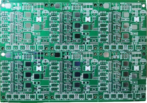
Table of Contents
Y&T TECHNOLOGY · MANUFACTURING SERVICES
HDI stack-up and via review
Use the technical information below to prepare a project-specific quotation.
- Include blind / buried via structure, microvia details, material stack-up and controlled impedance requirements.
- Include quantity, approved drawing revision, inspection requirements and target delivery date.
HDI construction review before quotation
Send with your request
- Provide the complete build-up, via structure and drill-span drawing.
- Identify microvias, buried vias, via-in-pad, filling and capping requirements.
- List fine-pitch interfaces, impedance targets, copper and critical registration tolerances.
Agree before the order starts
- Confirm the accepted via structure and process sequence with engineering.
- Agree reliability evidence, test coupons and inspection scope for the actual end use.
Include quantity, delivery destination and requested date. Your quotation identifies the accepted scope, exceptions, documentation and schedule.
If you’re in a fast-moving industry, you need to know about high density interconnect printed circuit boards. If your company isn’t using them now, they probably will be soon. If they aren’t, you can be sure your competitors are using them, so you need to learn about HDI PCBs and their benefits fast.
High density interconnect PCBs are a way of making more room on your printed circuit board to make them more efficient and allow for faster transmission. It’s relatively easy for most enterprising companies that are using printed circuit boards to see how this can benefit them.
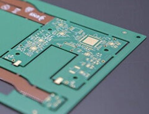
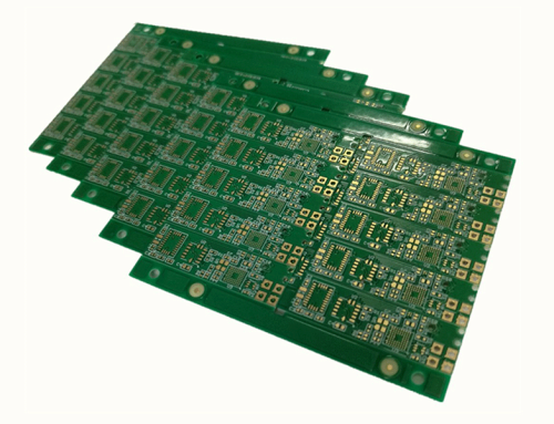
High density interconnect (HDI) PCBs represent one of the fastest-growing segments of the printed circuit board market. Because of its higher circuitry density, the HDI PCB design can incorporate finer lines and spaces, smaller vias and capture pads, and higher connection pad densities. A high-density PCB features blind and buried vias and often contains microvias that are .006 in diameter or even less.
Key HDI PCB Benefits
The evolution of high-density PCB technology has given engineers greater design freedom and flexibility than ever before. Designers using HDI high density interconnect methods now can place more components on both sides of the raw PCB if desired. In essence, an HDI PCB gives designers more space to work with, while allowing them to place smaller components even closer together. This means that a high-density interconnect PCB ultimately results in faster signal transmission along with enhanced signal quality.
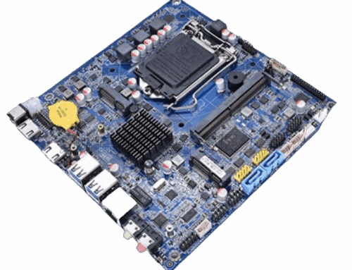
HDI PCB is widely used to reduce the weight and overall dimensions of products, as well as to enhance the electrical performance of the device. The high-density PCB is regularly found in mobile phones, touch-screen devices, laptop computers, digital cameras and 4G network communications. The HDI PCB is also prominently featured in medical devices, as well as various electronic aircraft parts and components. The possibilities for high-density interconnect PCB technology seem almost limitless.
HDI PCB Applications
HDI PCBs are appropriate for a wide range of industries. As mentioned above, you’ll find them in all types of digital devices, like smartphones and tablets, where miniaturization is key to the effective application of the product. You can also find high-density interconnect PCBs in automobiles, aircraft and other vehicles that rely on electronics.
One of the most critical areas where the high-density PCB is making huge inroads is in the medical arena. Medical devices frequently need small packages with high transmission rates that only HDI PCBs can supply. For example, an implant needs to be small enough to fit in the human body, but any electronics involved in that implant absolutely must efficiently allow for high-speed signal transmission. Here, the HDI PCB indeed is a godsend. HDI PCBs can also be useful in other medical equipment, like emergency room monitors, CT scans and much more.
No matter your industry, you’re probably already getting some ideas about how high-density interconnect PCBs can make the electronics you produce or use even better – get in touch with Y&T Technology to discuss it. We’ll let you know if you’re on the right track and help you decide exactly how beneficial an HDI PCB can be to your industry. Then, you can determine whether or not to take the next step.
No matter your industry, you’re probably already getting some ideas about how high-density interconnect PCBs can make the electronics you produce or use even better – get in touch with Y&T Technology to discuss it. We’ll let you know if you’re on the right track and help you decide exactly how beneficial an HDI PCB can be to your industry. Then, you can determine whether or not to take the next step.
High Density PCBs of Impeccable Quality
Over the course of a decade in business, Y&T Technology has established a hard-earned reputation for manufacturing PCBs of the highest quality. Our custom PCB manufacturing capabilities enable you to get the finest quality HDI PCBs at competitive prices without min order quantity requirement. Our team run design for manufacture check on your custom PCB file and consult with you to ensure it is ready for manufacturing and that your boards will meet your performance requirements. We also have an on-site quality control department to verify the finished product meet your high quality standards.
Provide the proposed HDI stack-up, build-up sequence and via strategy for engineering review. Feasibility is confirmed for the specific construction and order quantity:
For HDI constructions, include the proposed build-up sequence, via types, filled or capped via requirements, layer interconnections and expected quantities. Engineering confirms the manufacturable structure, process steps and production plan in the quotation.
Check our HDI PCB capabilities by reviewing the table found below:
| Feature | Information for engineering review |
| Quality Grade | Required IPC standard, revision, acceptance class and inspection scope agreed in the quotation. |
| Number of Layers | Provide the layer count and complete stack-up; engineering confirms the accepted construction. |
| Order Quantity | Provide initial and repeat-order quantities. Accepted batch size, panel utilization and charges are confirmed per project. |
| Build Time | Fabrication lead time and any accepted rush option are confirmed after material, construction, quantity and production review. This is separate from assembly and international transit. |
| Material | Specify the manufacturer, grade, datasheet revision and required material declarations; availability and substitutions require confirmation. |
| Board Size | Supply finished outline and panel drawing with units and dimensional tolerances; accepted dimensions are confirmed by engineering. |
| Board Thickness | Specify the finished thickness, stack-up and tolerance. Engineering confirms the achievable combination for your construction. |
| Copper Weight (Finished) | Specify starting and finished copper, units, layer location and tolerance. Feasibility is confirmed with the stack-up. |
| Min Tracing/Spacing | Provide trace and spacing requirements with units, copper weight and layer location; engineering confirms the design limits. |
| Solder Mask Sides | Specify mask sides, colour, openings, registration and any special acceptance requirements for review. |
| Solder Mask Color | Specify mask sides, colour, openings, registration and any special acceptance requirements for review. |
| Silkscreen Sides | Specify legend sides, colour, minimum text and registration requirements in the fabrication data. |
| Silkscreen Color | Specify legend sides, colour, minimum text and registration requirements in the fabrication data. |
| Surface Finish | Specify the finish or plating system, applicable standard, thickness and documentation required for the project. |
| Min Annular Ring | Identify drilled versus finished PTH or NPTH dimensions, units, tolerances and applicable stack-up for engineering review. |
| Min Drilling Hole Diameter | Identify drilled versus finished PTH or NPTH dimensions, units, tolerances and applicable stack-up for engineering review. |
| Max Exponents of Blind/Buried Vias | Identify the required special process, via construction, edge treatment or inspection. Engineering confirms availability and any tooling or cost impact. |
| Other Techniques | Identify the required special process, via construction, edge treatment or inspection. Engineering confirms availability and any tooling or cost impact. |
Quote HDI PCB manufacturing service now
Click below button to enter our HDI PCB quote page, then fill in your circuit spec;We will reply you as soon as possible by email with the price;If your high-density PCB project requires specifications not listed in the above table, feel free to contact us.
Contact us
WhatsApp: +86-13570802455
Wechat: +86-13570802455
Email: [email protected]