What is PCBA Tombstoning? Understanding the Manhattan Effect in SMT Assembly
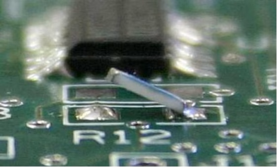
Table of Contents
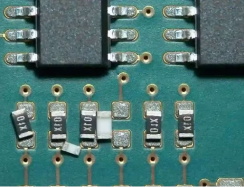
In the intricate world of electronics manufacturing, achieving perfection in printed circuit board assembly (PCBA) is a constant pursuit. Yet, even with advanced technology, certain defects can emerge, posing significant challenges to product reliability and performance. One such pervasive issue is “tombstoning,” a phenomenon that can leave small surface mount devices (SMDs) standing upright on the board, resembling miniature gravestones.
This defect, also known as the “Manhattan effect” or “drawbridge effect,” can lead to poor electrical connections, open circuits, and ultimately, a compromised electronic device. For anyone involved in PCBA processes—from engineers and manufacturers to quality control specialists—understanding the mechanics behind PCBA tombstoning and, more importantly, implementing effective prevention strategies is absolutely crucial. This comprehensive guide will delve into what tombstoning is, why it occurs, its impact, and practical methods to mitigate this frustrating defect, ensuring high-quality and reliable PCBAs.
1. What is PCBA Tombstoning?

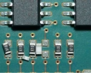
PCBA Tombstoning is a specific type of Surface Mount Technology (SMT) assembly defect where a small chip-type passive component, such as a resistor or capacitor, lifts off one of its solder pads during the reflow soldering process. Instead of lying flat, the component stands vertically on one of its terminations, hence its evocative name. This defect is predominantly observed in small passive components, particularly those in 0402, 0603, or even smaller 0201 package sizes, due to their light weight and delicate balance.
The visual characteristic of a component standing upright is unmistakable, often referred to as the “Manhattan effect” because the component’s vertical orientation resembles the skyline of Manhattan. Another descriptive term is the “drawbridge effect,” as the component lifts like a drawbridge. Regardless of the name, the outcome is an open circuit, rendering the component, and potentially the entire board, inoperable without costly rework. Preventing tombstoning is vital for ensuring the reliability and efficacy of printed circuit boards.
2. Why Does PCBA Tombstoning Occur? Unpacking the Root Causes
At its core, PCBA tombstoning is a consequence of uneven wetting forces during the reflow soldering process. Wetting describes the phenomenon where molten solder paste flows and creates a bond with both the component’s termination and the PCB pad. When the wetting forces on either end of a small component become imbalanced, one end may pull the component upwards while the other remains adhered to the board. Several factors contribute to this critical imbalance:
2.1 Uneven Solder Paste Application

The precision and consistency of solder paste deposition are paramount. If the volume of solder paste, its thickness, or its placement differs between the two pads of a component, it can lead to uneven wetting. Issues such as:
- Inconsistent Solder Volume:One pad receiving significantly more or less solder paste than the other.
- Solder Paste Viscosity:Incorrect viscosity can lead to poor stencil release or slumping, affecting deposit consistency.
- Stencil Design:Imperfect stencil apertures or misalignment can result in an unequal solder paste distribution.
These inconsistencies directly influence the surface tension forces that act on the component during reflow, creating an imbalance.
2.2 Reflow Profile Inaccuracies
The reflow soldering profile—which dictates the heating, soak, reflow, and cooling stages—is a critical determinant. An improperly tuned reflow profile can exacerbate PCBA tombstoning by:
- Rapid Heating Rates:If the temperature rises too quickly, one end of the component might melt and wet before the other, creating a strong pull.
- Insufficient Dwell Time:Not allowing enough time for both ends of the component and their respective solder pastes to reach the melting point uniformly can lead to one side wetting prematurely.
- Temperature Gradients:Significant temperature differences across the PCB, or even across the tiny component pads, can cause asynchronous solder melting.
Maintaining a gentle, consistent reflow profile is essential to ensure synchronous melting and wetting across both pads.
2.3 Component Placement Precision

Even the slightest misalignment of a component during the pick-and-place process can predispose it to PCBA tombstoning. If a component is placed slightly off-center, or if one end is slightly higher than the other, the molten solder paste will engage unevenly. The surface tension forces will then act more strongly on the better-aligned or lower end, pulling the component into an upright position.
2.4 Pad Design Inconsistencies
The design of the PCB pads themselves plays a crucial role. Differences in pad size, shape, or thermal mass between the two pads of a component can lead to asynchronous melting and wetting. For instance, a larger pad might take longer to heat, or a pad connected to a large ground plane might wick away heat more quickly, delaying solder melting on that side.
2.5 Component Characteristics
Certain characteristics of the components themselves can increase susceptibility to PCBA tombstoning:
- Smaller Package Sizes:As mentioned, tiny components like 0402 and 0201 are lighter and have smaller contact areas, making them more vulnerable to unbalanced surface tension forces.
- Component Weight/Mass:Extremely lightweight components offer less resistance to the upward pull of uneven solder wetting.
- Component Dimensions:Components with a high length-to-width ratio or irregular terminations can also be more prone.
Understanding these multifactorial causes is the first step toward implementing effective prevention strategies to ensure robust PCBA outcomes.
3. The Impact of Tombstoning on PCBA Quality
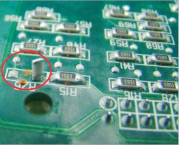
While PCBA tombstoning might appear as a minor aesthetic flaw, its implications for the functionality and reliability of electronic products are significant. It is far from a cosmetic issue; it represents a critical defect that can compromise the entire device. The primary impacts include:
- Electrical Connection Failure:The most direct consequence of a tombstoned component is an open circuit. Since one end of the component is not properly soldered, the intended electrical pathway is broken. This means the component cannot perform its function, leading to device malfunction.
- Reduced Product Reliability:A PCBA with tombstoned components will fail to meet its performance specifications. Such boards are prone to intermittent failures or complete operational failure, significantly impacting the end product’s reliability and lifespan. This can lead to increased warranty claims and customer dissatisfaction.
- Costly Rework and Scrap:When tombstoning occurs, the affected PCBAs require rework. This involves identifying the faulty component, desoldering it, and resoldering a new one correctly. Rework is a labor-intensive and time-consuming process that adds significant costs to production. Furthermore, if rework is not feasible or damages the board, the entire PCBA might have to be scrapped, leading to material waste and lost production time.
- Compromised PCBA Quality:Even if tombstoning can be fixed, the PCBA quality won’t be as good as the smoothly manufactured ones. Rework processes can introduce other stresses or slight imperfections that might not be immediately visible but could affect long-term reliability.
- Production Delays:The need for inspection, identification of defects, and subsequent rework directly translates into production delays. This can impact delivery schedules and market entry for new products.
Given these profound impacts, proactive prevention of PCBA tombstoning is not just a best practice but a fundamental requirement for achieving high-quality, reliable , and cost-effective electronic assemblies.
4. Preventing PCBA Tombstoning: Strategies for Flawless Assembly
Preventing PCBA tombstoning demands a synergistic approach, combining intelligent design choices with meticulous assembly practices. By addressing the root causes, manufacturers can significantly reduce or eliminate the occurrence of this defect. Here are key strategies:
4.1 Optimizing Solder Paste Application
The foundation of a good solder joint begins with precise solder paste deposition.
| Strategy | Description | Benefit |
| Correct Viscosity | Ensure solder paste viscosity is appropriate for the stencil and component size. | Enhances consistent stencil release and deposit shape. |
| Accurate Stencil Design | Design stencil apertures to provide balanced solder volume on both pads. Consider “home plate” or “oval” shapes for small components to improve wetting balance. | Promotes even solder paste deposit and symmetrical wetting forces. |
| Consistent Application | Regularly maintain and calibrate screen printers to ensure consistent pressure, speed, and separation distance. | Minimizes variations in solder paste volume and improves deposit quality. |
Proper viscosity and appropriate stencil designs can significantly enhance solder deposit consistency, reducing the likelihood of PCBA tombstoning.
4.2 Reflow Profile Management and Optimization
Carefully tuning the reflow oven profile is critical for synchronous solder melting and wetting.
| Strategy | Description | Benefit |
| Controlled Ramp Rates | Implement gradual ramp-up rates (preheat zones) to allow both the PCB and components to reach the desired temperature uniformly. | Minimizes thermal shock and ensures solder paste on both pads melts simultaneously. |
| Adequate Soak Time | Ensure a sufficient soak zone to activate flux and allow temperature equalization across the board. | Reduces temperature gradients, promoting uniform melting. |
| Optimized Peak Temperature & Dwell | Set peak reflow temperature and dwell time correctly to ensure complete wetting without overheating. | Achieves proper solder joint formation without premature wetting on one side. |
| Slow Cooling Rates | Avoid excessively fast cooling, which can introduce stress. | Allows for proper solidification and minimizes thermal stress. |
Accurate management of the reflow profile, especially for small components, is crucial for preventing uneven wetting.
4.3 Precision Component Placement

High-precision pick-and-place machines are essential for accurate component alignment.
- Accurate Alignment:Ensure that pick-and-place machines are calibrated and maintained to place components precisely centered on their respective pads.
- Vision Systems:Utilize advanced vision systems to verify component placement accuracy before reflow.
- Proper Nozzle Selection:Use appropriate vacuum nozzles to prevent component rotation or misalignment during placement.
Ensuring that component placement is precise is a fundamental technique to mitigate this risk.
4.4 Optimized Pad Design and PCB Layout
The design of the PCB pads directly influences thermal and wetting balance.
- Symmetrical Pad Design:Design pads to be as symmetrical as possible in terms of size and shape to ensure even heat distribution and solder wetting.
- Thermal Relief:For pads connected to large ground planes or power planes, incorporate thermal relief pads to prevent excessive heat sinking on one side. This helps balance the thermal mass of the two pads, promoting synchronous melting.
- Standardized Pad Dimensions:Adhere to IPC standards for pad geometries, especially for small passive components, to ensure consistency.
Adjusting the pad design or using components with slightly larger footprints can also help mitigate this risk.
4.5 Component Selection and Handling
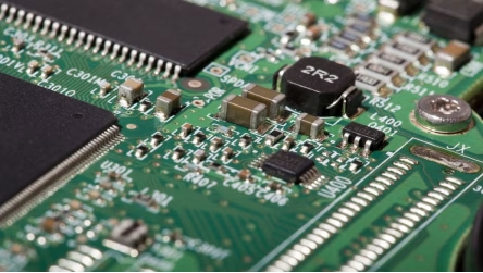
Choosing the right components and handling them properly can also play a role.
- Component Footprint:Where possible, consider using slightly larger footprint components if space allows, as they are less susceptible to PCBA tombstoning than ultra-small packages like 0201.
- Component Quality:Ensure components are of high quality, free from contamination, and have consistent termination finishes for optimal solderability.
- Proper Storage:Store components according to manufacturer specifications to prevent oxidation or moisture absorption, which can affect solderability.
For mid and high-end applications, selecting robust components is a key consideration.
4.6 Implementing Design for Manufacturing (DFM) Principles
Proactive DFM analysis early in the design phase can identify and address potential PCBA tombstoning risks before production begins. This involves a comprehensive review of component selection, pad design, and overall layout with manufacturing capabilities in mind. Turnkey PCB assembly manufacturers like yt-electronic emphasize systematic approaches and rich DFM experience to prevent PCBA tombstoning from occurring.
By integrating these strategies, manufacturers can significantly reduce the incidence of tombstoning, leading to higher quality, more reliable, and more cost-effective PCBA production.
5. PCBA Tombstoning FAQs
PCBA tombstoning is also widely known as the “Manhattan effect” or the “drawbridge effect” due to the component’ s upright appearance after reflow soldering.
Small chip-type passive components, such as resistors and capacitors, especially in smaller package sizes like 0402, 0603, and 0201, are most prone to PCBA tombstoning because their low mass makes them highly susceptible to unbalanced surface tension forces during reflow.
Yes, tombstoned components can often be reworked by carefully desoldering and resoldering a new component. However, rework adds significant cost and time, and the quality of a repaired PCBA may not be as robust as one manufactured flawlessly initially.
6. Summary
PCBA tombstoning, also known as the Manhattan effect or drawbridge effect, is a critical SMT assembly defect where small components stand upright on the PCB. This phenomenon primarily results from uneven wetting forces during reflow soldering, stemming from factors like inconsistent solder paste application, inaccurate reflow profiles, imprecise component placement, and imbalanced pad designs.
The consequences are severe, leading to open circuits, device malfunction, reduced product reliability, and costly rework or scrap. Preventing PCBA tombstoning requires a multi-faceted approach, including optimizing solder paste consistency, meticulously controlling reflow profiles, ensuring high-precision component placement, designing symmetrical pads with proper thermal relief, and making informed component selections. By adopting these comprehensive strategies and implementing robust Design for Manufacturing (DFM) principles, manufacturers can achieve flawless PCB assembly, enhance product quality, and significantly reduce production costs.
Key Takeaways
- Tombstoning is a critical PCBA defect where small components stand vertically, causing open circuits.
- Uneven wetting forces during reflow soldering are the primary cause, influenced by solder paste, reflow profile, and placement.
- The defect significantly impacts product reliability, leading to malfunction and costly rework.
- Prevention involves optimizing solder paste (viscosity, stencil), precise reflow profiles, accurate component placement, and balanced pad design.
- Implementing DFM principles early in the design phase is crucial for proactive tombstoning prevention.
Contact us
WhatsApp: +86-13570802455
Wechat: +86-13570802455
Email: [email protected]