PCB Assembly Process
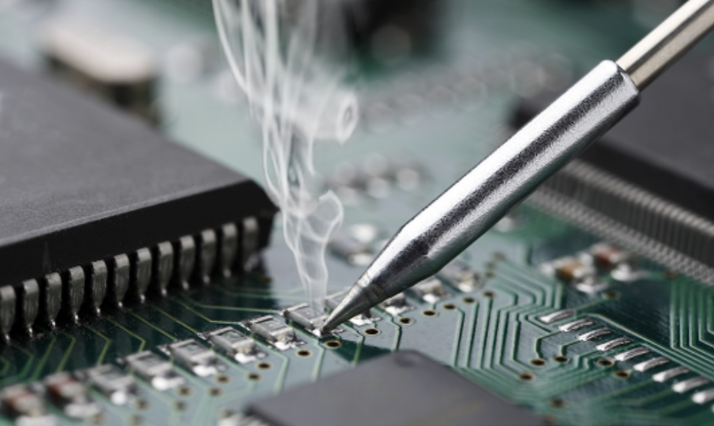
Table of Contents
PCB ASSEMBLY PROCESS · FROM RELEASED FILES TO ASSEMBLED BOARDS
PCB assembly adds electronic components to a fabricated circuit board. Bare-board fabrication and assembly are separate stages, even when they are purchased together. The sequence below explains a typical build; the actual route depends on the design, supplied materials and agreed inspection and test scope.
For a quotation covering your project, explore our PCB assembly services.
PCB assembly process, step by step
1. Review the released design and build scope
Start with matching revisions of the fabrication data, BOM, placement file and assembly drawings. Identify DNP positions, orientation notes, build quantity, material supply responsibilities and required tests. For an initial design build, define the evaluation questions in your prototype PCB assembly request.
2. Prepare bare boards and source components
The bare PCB provides the copper interconnections, drilled holes and surface finish specified by the design. Component sourcing uses the BOM, including exact manufacturer part numbers and suffixes. Material availability, customer-supplied items and proposed alternatives need to be resolved against the approved build.
If you need boards and components coordinated with assembly, see full turnkey PCB assembly for the purchasing information to include.
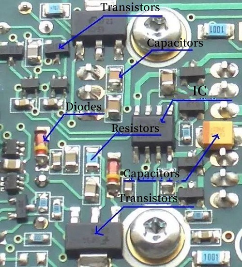
3. Apply solder paste and place SMT components
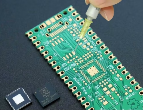
For a conventional SMT process, solder paste is deposited on the appropriate pads and surface-mount components are placed according to the released data. Paste deposits, component identity, position and polarity are process checks before and after soldering as appropriate to the build.
4. Reflow solder the SMT assembly
During reflow, a controlled temperature profile heats the populated board so the solder paste melts and wets the PCB pads and component terminations. Controlled cooling forms the solder joints. The profile must suit the selected materials, components and assembly.
5. Insert and solder through-hole components where required
Through-hole parts have leads inserted into board holes. Wave soldering brings the relevant joints into contact with a wave of molten solder. Depending on board layout, components and production needs, through-hole assembly may instead use selective or manual soldering. The appropriate route is agreed for the project.
6. Inspect, program and test to the agreed scope
Inspection and functional testing answer different questions. Define the required inspection coverage, acceptance criteria, programming version and functional-test procedure. Supply fixture details and pass/fail limits where needed so the quotation can identify preparation work and required records.
7. Separate panels, complete final checks and pack
Where boards are assembled in a panel, separation and handling must be considered with the design and test plan. Review the PCB panel requirements for assembly before releasing fabrication data. Confirm final board identification, packing and shipment instructions for the order.
Common assembly issues to review
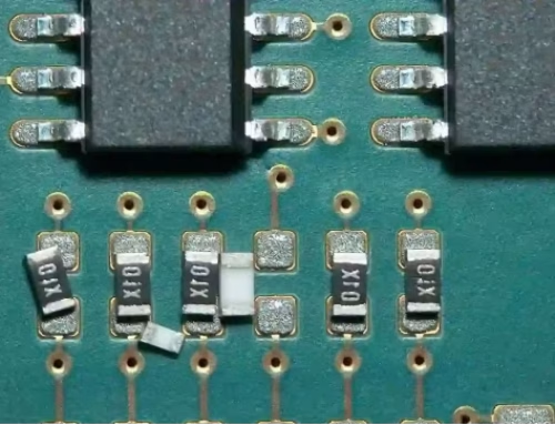
Component identity or orientation errors, misalignment and solder-joint defects require different checks and corrective actions. A clear released data package and agreed acceptance criteria help define what to inspect and how to handle a nonconformance.
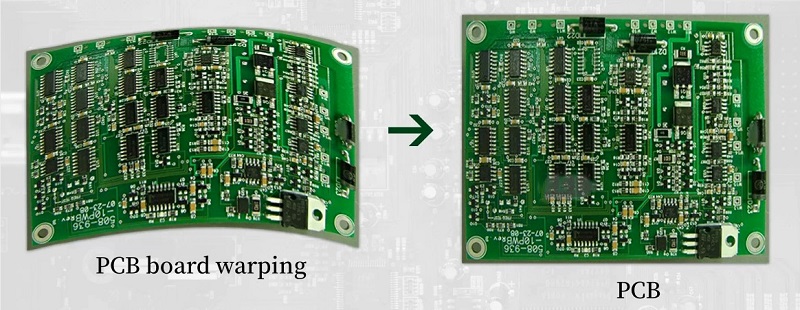
Board condition and handling
Board distortion and damage should be considered alongside the material, manufacturing, handling and assembly process. Identify critical flatness or mechanical requirements in the project documentation.
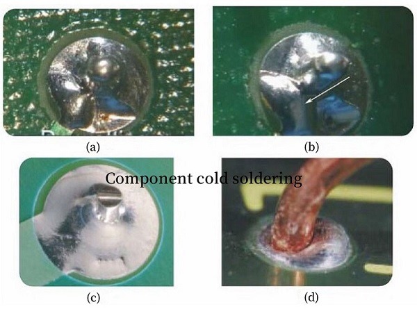
Solder-joint and placement findings
Record the affected location, observed condition and applicable acceptance requirement. Separate observations from a confirmed root cause, and agree any rework or design change before the affected work proceeds.
Choose the service that matches your build
- Prototype assembly for a first build and design evaluation.
- Turnkey assembly when the request includes boards, BOM sourcing and assembly.
- Low-volume, high-mix assembly for repeat batches or multiple board variants.
Turn your design package into an assembly RFQ
Send the information you have: board and panel files, an editable BOM with exact part numbers, placement data, quantity, delivery country and required inspection or tests. Identify missing files or open questions so they can be clarified before a production quote is confirmed.
Request my PCB assembly quoteDownload the RFQ & BOM worksheet
The blank Excel worksheet is optional (XLSX, 8 KB). Your existing BOM format is welcome. Include a separate dimensioned panel drawing if panelization is part of your request.
For NDA requirements or a question before sharing files, contact our team.
Technical reading
For the general soldering principles, see the equipment manufacturer’s descriptions of Ersa reflow soldering and Ersa wave soldering. These references explain the processes; equipment selection and the manufacturing route for an order are confirmed separately.
Contact us
WhatsApp: +86-13570802455
Wechat: +86-13570802455
Email: [email protected]