HEF4071BP HEF4071BP,652 NXP Logic OR Gate IC Guide
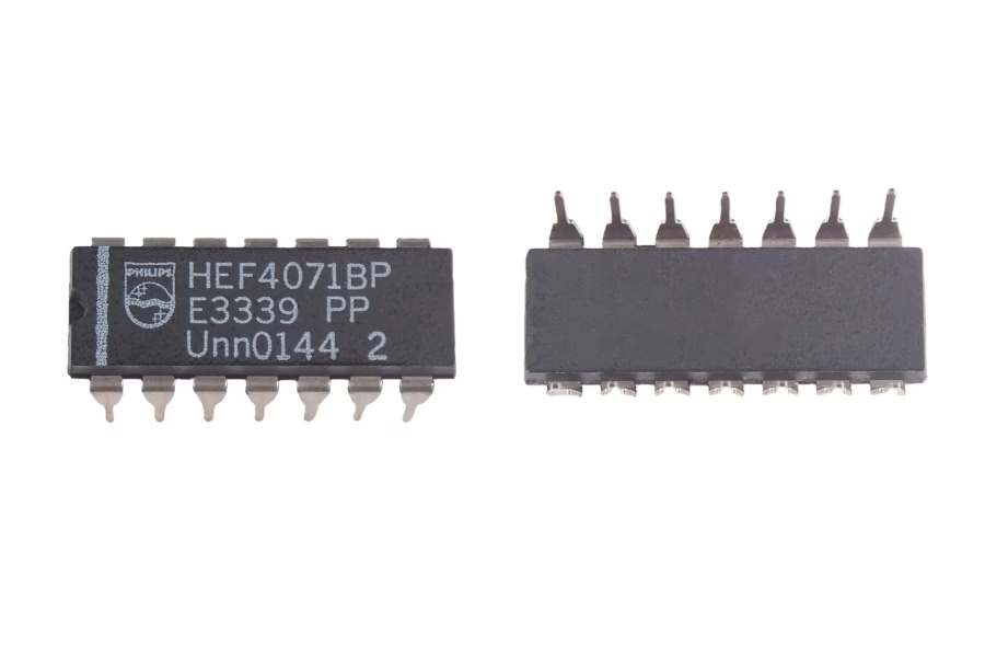
Table of Contents
- 1. Understanding the OR Gate: Core Digital Logic
- 2. NXP HEF4071BP,652: A Deeper Dive into the Quad OR Gate IC
- 3. The Price Range of HEF4071BP HEF4071BP,652
- 4. Key Features and Electrical Specifications
- 5. HEF4071BP HEF4071BP,652 Datasheet Download
- 6. Versatile Applications of the HEF4071BP,652
- 7. Designing with the HEF4071BP,652
- 8. The 4000-Series CMOS Advantage
- 9. Sourcing Your HEF4 071BP,652
- 10. HEF4071BP HEF4071BP,652 FAQs
- 11. Summary
- Key Takeaways
In the vast landscape of digital electronics, integrated circuits (ICs) serve as the fundamental building blocks that power everything from simple hobby projects to complex industrial automation systems. Among the myriad of ICs, logic gates are the foundational components that perform basic Boolean operations. Today, we’re diving deep into a workhorse of the 4000-series CMOS logic family: the NXP HEF4071BP, commonly found as the HEF4071BP,652.
This comprehensive guide will demystify the HEF4071BP,652, explaining its core function as a quad 2-input OR gate, detailing its specifications , exploring its versatile applications, and providing practical insights for engineers and enthusiasts alike. Whether you’re designing a new digital circuit, troubleshooting an existing system, or simply looking to expand your knowledge of essential logic ICs, understanding the HEF4071BP,652 is a crucial step.
1. Understanding the OR Gate: Core Digital Logic
Before we dissect the HEF4071BP,652, let’s briefly revisit the concept of an OR gate, which is one of the three fundamental logic gates (AND, OR, NOT). An OR gate performs a logical disjunction operation. Its output is TRUE (logic 1, or high voltage) if at least one of its inputs is TRUE. If all inputs are FALSE (logic 0, or low voltage), then and only then is the output FALSE.
In digital circuits, this translates to: If input A is high OR input B is high (or both are high), the output will be high. This simple yet powerful logic is essential for decision-making and data flow control within digital systems. The Boolean expression for a 2-input OR gate is A + B = Y, where Y is the output.
Here’s a simple truth table for a 2-input OR gate:
| Input A | Input B | Output Y |
| 0 | 0 | 0 |
| 0 | 1 | 1 |
| 1 | 0 | 1 |
| 1 | 1 | 1 |
2. NXP HEF4071BP,652: A Deeper Dive into the Quad OR Gate IC
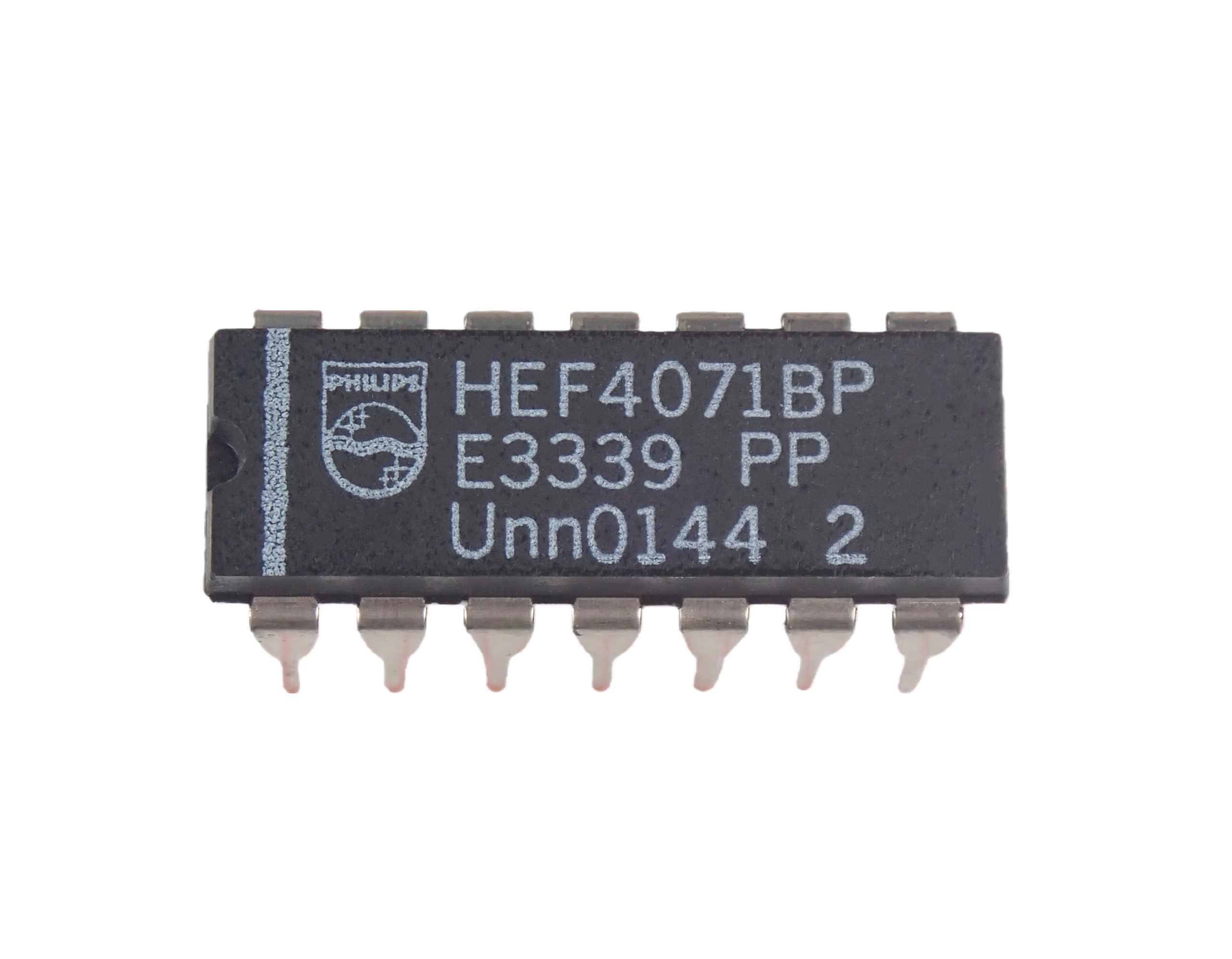
The NXP HEF4071BP,652 is a highly reliable integrated circuit designed to provide four independent 2-input OR gates within a single package. NXP Semiconductors, a leading player in the semiconductor industry, manufactures this component as part of their extensive range of logic ICs. The “BP” in HEF4071BP typically refers to a specific package type (e.g., PDIP), while “BP,652” indicates packaging format, but they share the same core functionality as a quad 2-input OR gate.
This IC belongs to the HEF4000 series, a family of CMOS(Complementary Metal-Oxide-Semiconductor) logic devices known for their low power consumption and wide operating voltage range, making them suitable for a broad spectrum of digital applications. The “quad 2-input” configuration means that a single HEF4071BP,652 chip can handle four separate OR logic operations simultaneously, saving board space and simplifying circuit design.
3. The Price Range of HEF4071BP HEF4071BP,652
According to the latest market conditions, the price range for HEF4071BP or HEF4071BP,652 is approximately USD0.634 – USD1.409 per piece. The specific price may vary depending on the following factors:
Purchase quantity (bulk purchases typically offer more favorable unit prices)
Supplier and regional differences
We are very strong on Electronic Components Distribution for more than 12 years. We can make sure that all the components from our company are 100% Original and New! Please feel free to contact us if you have any needs.
4. Key Features and Electrical Specifications
The HEF4071BP,652 boasts features that make it a robust choice for various digital applications . Its CMOS design ensures efficient performance, particularly where power consumption is a concern. Let’s look at some of its critical specifications:
| Feature | Specification (HEF4071BP,652) | Benefit |
| Logic Type | OR Gate | Performs basic logical disjunction |
| Number of Gates | 4 (Quad) | Multiple OR operations in one chip |
| Number of Inputs per Gate | 2 | Standard configuration for various logic tasks |
| Output Current (Low) | 3.6mA | Sufficient drive for many loads |
| Max Propagation Delay @ 15V, 50pF | 35ns | Relatively fast operation for CMOS logic at higher voltages |
| Typical Propagation Delay | 50ns | Standard speed for general-purpose applications |
| Operating Voltage Range | Typically 3V to 15V (or wider, depending on specific datasheet variant) | Wide compatibility with different power supplies |
| Package Type | 14-DIP | Through Hole |
| Family | HEF4000 series (CMOS) | Low power consumption, high noise immunity |
The propagation delay figures indicate the time it takes for a change at the input to reflect at the output. While 4000-series CMOS devices are generally slower than their TTL (Transistor-Transistor Logic) or 74HC counterparts, their ultra-low power consumption and wide voltage tolerance often make them preferable for battery-powered or robust industrial applications.
5. HEF4071BP HEF4071BP,652 Datasheet Download
- HEF4071BP HEF4071BP,652 Datasheet: HEF4071BP
6. Versatile Applications of the HEF4071BP,652
The humble OR gate, exemplified by the HEF4071BP,652, finds its way into countless digital circuits. Its ability to perform logical decision-making based on multiple inputs makes it incredibly versatile. Here are some common applications:
Condition Monitoring and Alarm Systems: Imagine a system that triggers an alarm if “door open” OR “window open” OR “motion detected.” An OR gate is perfect for consolidating these conditions into a single alarm trigger.
Data Selectors and Multiplexers: While dedicated multiplexer ICs exist, OR gates can be used in combination with other gates to create simple data routing or selection logic, enabling different data paths based on control signals.
Security Systems: Similar to alarm systems, OR gates can combine inputs from multiple sensors (e.g., pressure sensor, infrared sensor) to activate a security measure if any one of them is triggered.
Control Logic: In industrial control systems, the HEF4071BP,652 can be used to control actuators or motors based on various operational conditions. For example, a motor might start if “manual override” OR “automatic mode enabled” OR “safety interlock cleared.”
Logic Level Translation: Due to its wide operating voltage range, the HEF4071BP,652 can sometimes be part of circuits that interface between systems operating at different voltage levels, though dedicated level shifters are often more appropriate for complex designs.
Simple Decoders: When combined with AND and NOT gates, OR gates contribute to decoding logic, such as enabling specific functions when certain input combinations are met.
7. Designing with the HEF4071BP,652
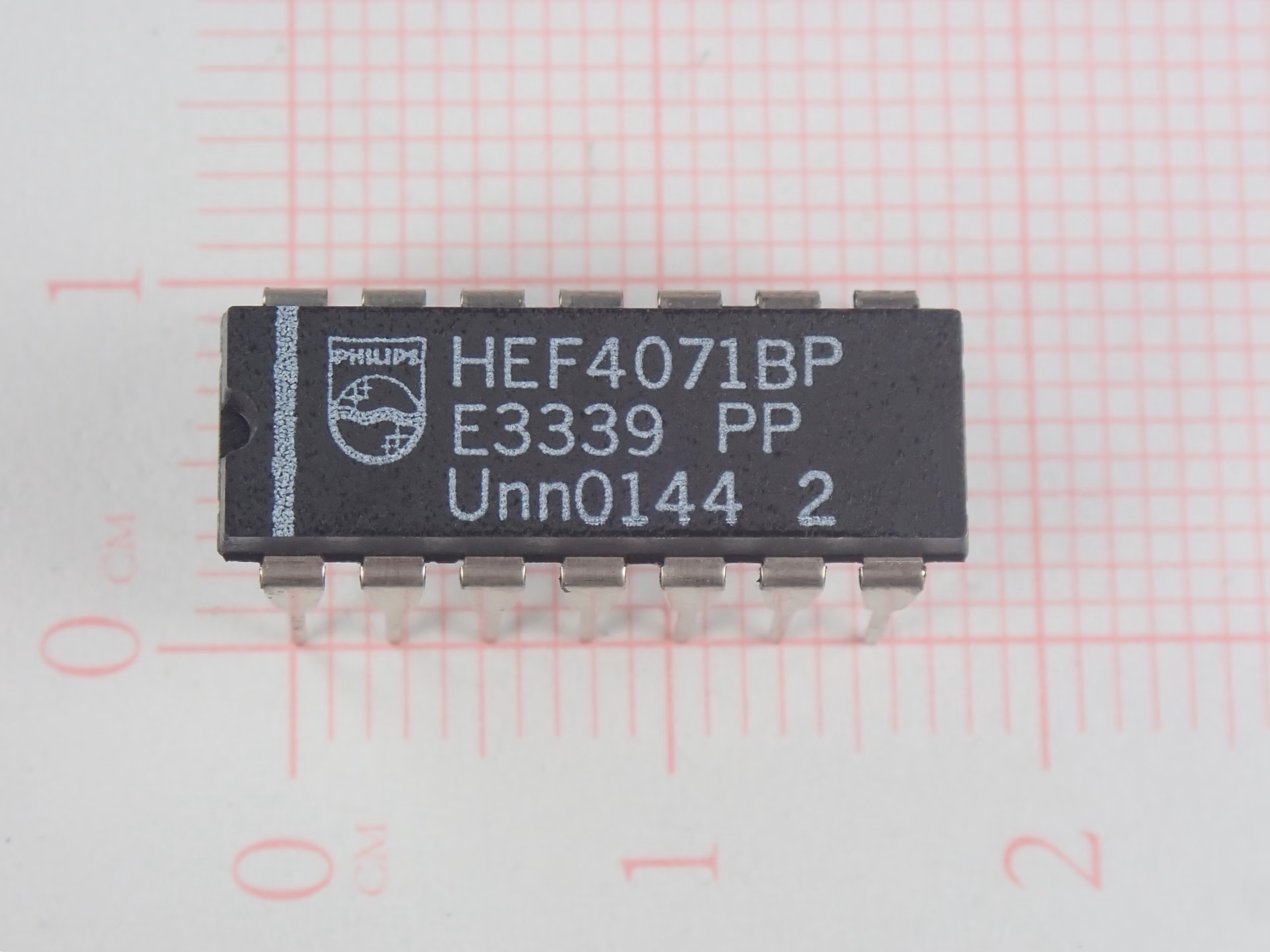
When incorporating the NXP HEF4071BP,652 into your designs, several factors should be considered to ensure optimal performance and reliability:
Power Supply and Decoupling
The HEF4071BP,652 operates across a wide voltage range, typically from 3V to 15V. Always refer to the specific NXP datasheet for the exact recommended operating conditions. It is crucial to use a stable power supply and include a decoupling capacitor (e.g., 0.1µF ceramic) placed close to the IC’s VDD and VSS pins. This capacitor helps to filter out noise on the power lines and provide instantaneous current during switching transients.
Unused Inputs
A common pitfall with CMOS logic is leaving unused inputs floating. Floating inputs can pick up ambient electrical noise, causing unpredictable behavior and increased power consumption due to indeterminate logic states. For unused inputs on the HEF4071BP,652, it’s best practice to tie them to either VDD (high) or VSS (low), depending on the desired logic state or if they are part of an unused gate, tie them to VSS to disable that gate’s output.
Output Loading
While the HEF4071BP,652 has a respectable output current capability (e.g., 3.6mA low output current), it’s important not to exceed its maximum ratings. Overloading an output can lead to incorrect voltage levels, increased propagation delays, or even permanent damage to the IC . When driving higher current loads or multiple gates, consider using a buffer or a dedicated driver IC.
Propagation Delay and Speed
The propagation delay of 35-50ns is typical for the 4000-series CMOS family. For high-speed applications, this might be a limiting factor. If your design requires faster switching speeds, consider looking into faster logic families like the 74HC series, which offers similar gate types but with significantly reduced delays. However, for most general-purpose or low-frequency digital designs, the HEF4071BP,652’s speed is more than adequate.
8. The 4000-Series CMOS Advantage
The HEF4071BP,652 is a part of the CD4000 (or HEF4000 for NXP) series of CMOS logic ICs. This family was introduced as a low-power, wide-voltage alternative to the earlier 7400 series TTL logic. Key advantages of the 4000-series include:
Low Power Consumption: CMOS devices consume very little static power, making them ideal for battery-powered devices or applications where energy efficiency is critical. Power consumption primarily increases during switching.
Wide Operating Voltage Range: The ability to operate from 3V to 15V (and sometimes up to 18V) allows for greater flexibility in power supply design and compatibility with various other components .
High Noise Immunity: CMOS logic typically has higher noise immunity compared to TTL, meaning it’s less susceptible to spurious signals, which is beneficial in noisy industrial environments.
While newer , faster CMOS families like the 74HC series and 74AC/74ALS exist, the 4000-series continues to be relevant for its robust nature and specific characteristics.
9. Sourcing Your HEF4 071BP,652
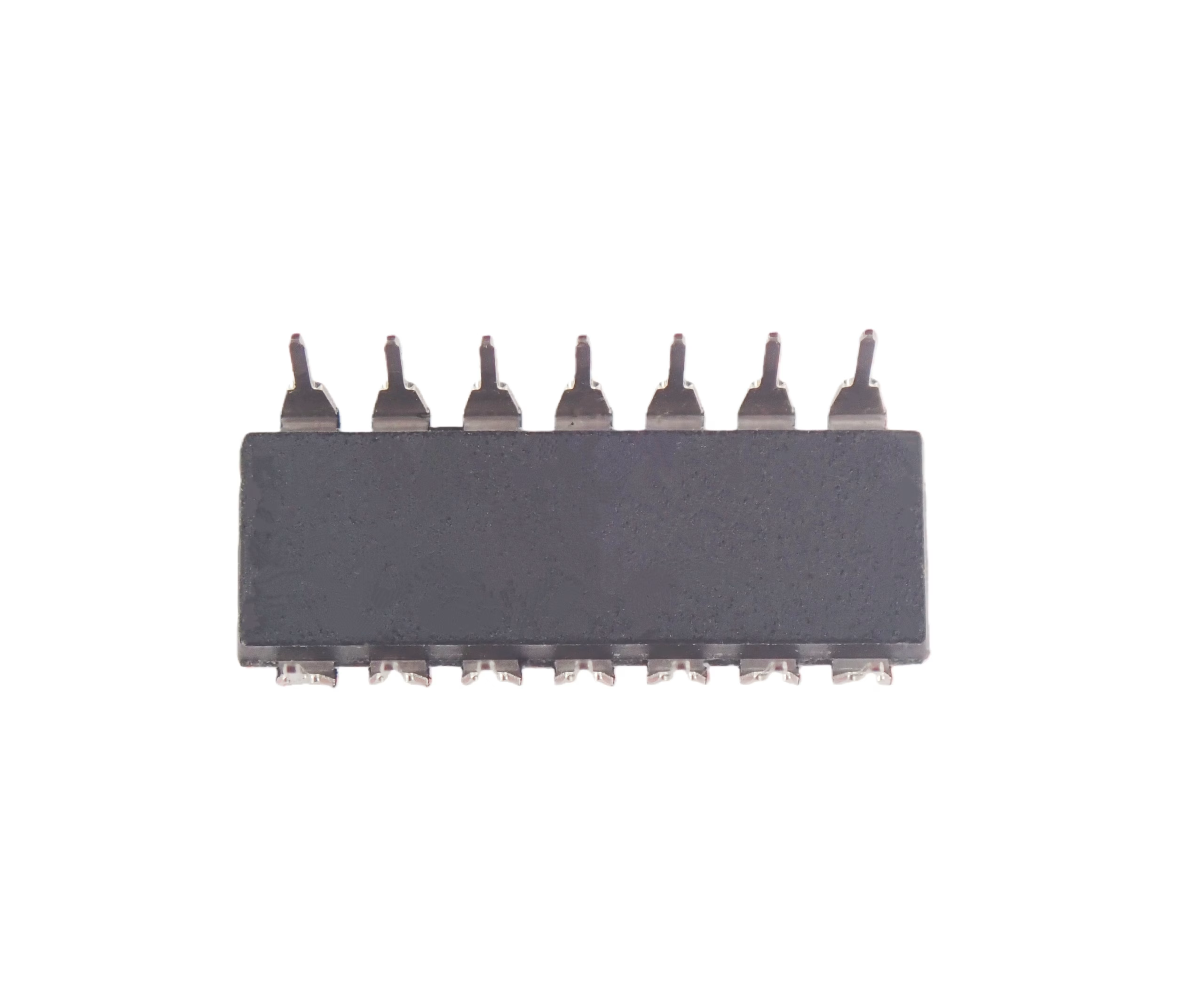
When you need to acquire the NXP HEF4071BP,652, it’s important to source from authorized distributors to ensure authenticity and quality. Major electronics distributors like DigiKey are reliable channels for purchasing these components. Another source, yt-electronic.com, also provides specific details for the HEF4071BP,652, confirming NXP Semiconductors as the brand and providing key specifications for easy ordering. Always check for current availability and pricing from these reputable suppliers.
10. HEF4071BP HEF4071BP,652 FAQs
The primary difference lies in the package type. “BP” typically refers to a through-hole PDIP (Plastic Dual In-line Package), while “BP,652” indicates a small outline Integrated Circuit package with specific tape-and-reel packaging. Functionally, the core quad 2-input OR gate logic remains the same.
Yes, absolutely. The HEF4071BP,652, being a 4000-series CMOS device, has a wide operating voltage range, typically from 3V up to 15V (or even 18V). A 5V power supply is well within its specified operating range.
For stable operation and to prevent noise pickup or increased power consumption, all unused inputs of any CMOS logic gate, including the HEF4071BP,652, should be tied to either VDD (high) or VSS (ground). Do not leave them floating.
11. Summary
The NXP HEF4071BP,652 (and its general HEF4071BP variant) stands as a foundational component in the world of digital electronics. As a quad 2-input OR gate IC, it performs essential logical disjunction operations with the benefits of the 4000-series CMOS family: low power consumption, wide operating voltage, and high noise immunity. From simple alarm circuits to more complex control systems, its versatility makes it an invaluable tool for designers. Understanding its specifications , proper design practices, and reliable sourcing ensures that this robust IC continues to play a vital role in countless electronic innovations.
Key Takeaways
- The NXP HEF4071BP,652 is a Quad 2-Input OR Gate IC from the reliable 4000Bseries CMOS logic family.
- It offers low power consumption, a wide operating voltage range (e.g., 3V to 15V), and high noise immunity.
- Key specifications include a typical propagation delay of 50ns and an output current (low) of 3.6mA.
- Common applications span condition monitoring, alarm systems, data selection, and general control logic.
- Always tie unused inputs to VDDor VSS, use decoupling capacitors, and avoid exceeding output current limits for optimal circuit performance.
Contact us
WhatsApp: +86-13570802455
Wechat: +86-13570802455
Email: [email protected]