PCB Vias: Essential Connections for Modern Circuit Boards
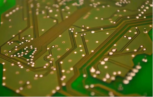
Table of Contents
Printed Circuit Boards (PCBs) are the backbone of almost all modern electronics. As designs become more complex and miniaturized, the need to connect multiple layers within a PCB efficiently and reliably becomes paramount. This is where vias come into play. A PCB via is essentially a plated hole that creates an electrical connection between different layers of a multi-layer PCB, acting as a vertical bridge for signals, power, and ground.
Understanding the various types of vias, their applications, and design considerations is crucial for any PCB designer aiming for optimal performance, density, and manufacturability. This guide delves into the fundamental aspects of PCB vias, offering a comprehensive overview of their classification, construction, and critical design factors.
1. What is a PCB Via?
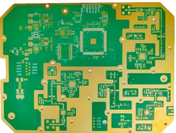
At its core, a PCB via is a small, drilled hole in a PCB that is subsequently plated with a conductive material, typically copper. This plating ensures that electrical signals can travel vertically between the copper traces on different layers of the board. Without vias, multi-layer PCBs would be impossible, severely limiting the complexity and functionality of electronic devices.
Vias serve several critical functions:
- Electrical Connectivity:The primary role is to create electrical pathways between distinct copper layers.
- Thermal Management:Certain vias, known as PCB thermal via, are specifically designed to conduct heat away from components, dissipating it into internal copper planes or other layers.
- Mechanical Support:While not their primary function, plated through-holes (which include vias) can also provide mechanical support for components, especially in through-hole mounting.
2. What are the Types of PCB Vias?
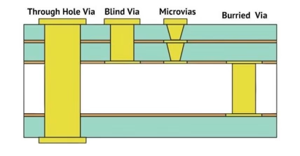
Not all vias are created equal. Depending on the specific requirements of the PCB design – such as layer count, routing density, signal integrity, and cost–different types of vias are employed. The main classifications are based on how they connect the layers :
2.1 Through Hole Vias (Through Board Vias)
The most common and simplest type, a through hole via extends completely through all layers of the PCB , from the top outer layer to the bottom outer layer. These are mechanically drilled and then plated with copper.
- Characteristics:Visible from both sides of the board. Easiest to manufacture, making them the most cost-effective option.
- Applications:General interconnects, power and ground connections, component mounting for through-hole components.
- Limitations:Consume valuable routing space on all layers they pass through, which can be inefficient for high-density interconnect (HDI) designs.
2.2 Blind Vias
A blind via PCB connects an outer layer of the PCB to one or more inner layers, but does not pass through the entire board. It is “blind” because it cannot be seen from the opposite outer side of the board.
- Characteristics:Improves routing density by only occupying space on the layers it connects. Often created using laser drilling, especially for smaller dimensions.
- Applications:High-density designs where space is at a premium, enabling more routing channels on the outer layers.
- Limitations:More complex to manufacture than through hole vias, leading to higher costs. Requires precise depth control during drilling.
2.3 Buried Vias
A PCB buried via connects two or more inner layers of the PCB without reaching any outer layers. It is completely “buried” within the board structure and is not visible from either surface.
- Characteristics:Offers the highest routing density, freeing up both outer layers for component placement and routing. Can be mechanically or laser drilled.
- Applications:Extremely high-density, multi-layer PCBs , often found in complex consumer electronics, server boards, and medical devices.
- Limitations:The most expensive and complex to manufacture, as they require drilling and plating individual sub-laminates before the final board stack-up.
2.4 Microvias
A microvia PCB is a very small via, typically with a diameter of 150 microns (6 mil) or less . These are almost exclusively formed by laser drilling and are crucial for High-Density Interconnect (HDI) PCBs.
- Characteristics:Extremely small size allows for ultra-fine pitch component connections and increased routing density. Improved electrical performance due to lower parasitic capacitance and inductance, beneficial for high-frequency signals.
- Applications:HDI boards, smartphones, tablets, wearables, high-speed data communications equipment.
- Types: Microvias can be blind or stacked (multiple microvias on top of each other), but are rarely through-hole in the traditional sense.
The combination of blind and buried vias, often including microvias, is known as blind buried vias technology, which represents the pinnacle of PCB miniaturization and density.
2.5 Thermal Vias
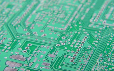
Unlike other vias primarily focused on electrical signal transmission, a PCB thermal via is designed to conduct heat. They are strategically placed under heat-generating components (like power ICs) to draw heat away from the component and distribute it to internal ground planes or other heat-sinking layers.
- Characteristics:Often placed in an array or grid pattern. They may be filled with a thermally conductive material (e.g., copper paste) to enhance heat transfer and prevent solder wicking during assembly.
- Applications:Power electronics, LED lighting, motor drivers, and any application where component temperature management is critical.
- Design Considerations:Number and size of thermal vias impact efficiency. Filling them is often recommended for optimal performance.
3. Via Filling and Capping
Filled vias PCB refers to the process of filling vias with a non-conductive or conductive material. This practice serves several important purposes:
- Prevents Solder Wicking:Without filling, molten solder can flow into the via during assembly, leading to insufficient solder joints on pads or even short circuits.
- Improves Reliability:Filling and capping vias creates a flat, planar surface over the via, which is essential for mounting fine-pitch components (like BGAs) directly over vias without creating reliability issues.
- Enhances Thermal Performance:As mentioned, thermal vias are often filled with thermally conductive paste to maximize heat dissipation.
- Increases Mechanical Strength:Filled vias can sometimes offer additional structural integrity to the board, especially under repeated thermal cycling.
Common filling materials include non-conductive epoxy resin, copper paste, or even silver-filled conductive epoxy. After filling, vias are often “capped” or “plated over” with copper to ensure a smooth surface for soldering.
4. Design Considerations for PCB Vias
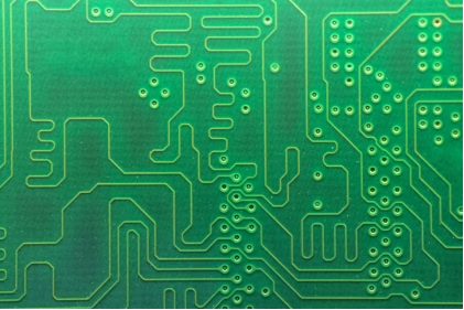
Effective via design goes beyond merely selecting a type. Several factors must be considered to ensure optimal PCB performance and manufacturability:
- Aspect Ratio:This is the ratio of the drill depth to the drill diameter. A higher aspect ratio (deeper, smaller diameter) is more challenging to plate reliably and can increase manufacturing costs. Standard limits apply for different manufacturers.
- Impedance Control:For high-speed signals, vias can introduce discontinuities that affect signal integrity. Careful design, including stub length reduction (back-drilling) and specific pad/anti-pad dimensions, is necessary to minimize impedance mismatches.
- Via-in-Pad Technology:This technique places a via directly within a Surface Mount Device (SMD) pad. It is often used for fine-pitch BGAs to save space and improve routing. These vias are typically filled and capped to ensure a flat soldering surface.
- Annular Ring:The copper pad around the drilled hole. A sufficient annular ring is critical for reliable electrical connection and to prevent drill breakout, where the drill wanders outside the pad.
- Current Carrying Capacity:Larger vias can carry more current. For power paths, multiple vias or larger diameter vias might be required to minimize voltage drop and heat generation.
- Manufacturing Capabilities:Always consider the capabilities of your chosen PCB fabricator. Not all manufacturers can produce all types of vias or achieve very small drill sizes and high aspect ratios.
5. Standard PCB Via Sizes
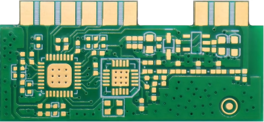
The standard PCB via sizes can vary slightly between manufacturers and design rules, but generally refers to common dimensions used for reliable production. Vias are typically defined by their drill diameter and the outer pad diameter.
Below is a general guideline for typical ranges, though specific design rules (e.g., 6/12 mil for drill/pad) are often specified:
| Via Type | Typical Drill Diameter (mm/mil) | Typical Pad Diameter (mm/mil) | Notes |
| Through Hole Via | 0.25 – 0.60 mm (10 – 24 mil) | 0.50 – 1. 0 mm (20 – 40 mil) | Most common, larger sizes for higher current. |
| Blind/Buried Via | 0.15 – 0.30 mm (6 – 12 mil) | 0.35 – 0.60 mm (14 – 24 mil) | Smaller than through-hole for density. |
| Microvia | 0.05 – 0.15 mm (2 – 6 mil) | 0.25 – 0. 35 mm (10 – 14 mil) | Laser drilled, for HDI applications. |
It’s important to note that the minimum drill size and aspect ratio are critical manufacturing parameters. For instance, a common manufacturing capability might limit the aspect ratio to 10:1 for mechanical drills and 1:1 for laser drills (microvias).
6. Choosing the Right PCB Vias
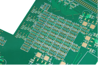
Selecting the appropriate via type is a critical design decision influenced by several factors:
- Density Requirements:For very high-density boards, microvias, blind vias, and buried vias are essential to maximize routing space. For simpler boards, through hole vias are often sufficient.
- Signal Integrity:High-speed and high-frequency designs benefit from smaller vias (microvias) to reduce parasitic effects. Blind and buried vias also help minimize stub length, which improves signal quality.
- Cost:Through hole vias are the least expensive. Blind and buried vias, especially microvias, significantly increase manufacturing costs due to more complex drilling, plating, and lamination processes.
- Manufacturing Capabilities:Always verify that your chosen PCB fabricator can reliably produce the specific via types and sizes required by your design.
- Thermal Management:If components generate significant heat, incorporating thermal vias becomes a priority.
7. PCB Vias FAQs
A blind via connects an outer layer to an inner layer but doesn’t go all the way through the board. A buried via connects two or more inner layers and is completely hidden within the PCB structure.
Microvias allow for extremely high routing density and finer pitch component connections, crucial for miniaturized devices like smartphones. They also offer improved electrical performance for high-frequency signals due to their small size.
Via-in-pad places a via directly within a component ‘s solder pad. It’s used to save space, especially with fine-pitch BGAs, and allows for more efficient routing. These vias are usually filled and capped to ensure a flat, reliable soldering surface.
No. Via sizes are constrained by manufacturing capabilities (minimum drill diameter, aspect ratio) and design rules. Using standard or commonly accepted sizes within your fabricator’s capabilities ensures reliability and cost-effectiveness.
8. Summary
PCB vias are indispensable elements in the design and manufacturing of multi-layer printed circuit boards, acting as critical vertical interconnects. From the simple and cost-effective through hole via to the advanced microvias used in High-Density Interconnect (HDI) boards, each type serves specific design requirements related to routing density, signal integrity, and thermal management. Blind vias and buried vias offer significant advantages in space optimization, while thermal vias are essential for managing heat in power-intensive applications.
The choice and implementation of vias require careful consideration of factors like aspect ratio, impedance control, manufacturing capabilities, and cost. Understanding these elements allows designers to create robust, high-performance, and manufacturable PCBs that meet the demands of increasingly complex electronic devices.
Key Takeaways
- Vias are essential:They provide critical electrical, and sometimes thermal, connections between layers in multi-layer PCBs.
- Diverse Types for Diverse Needs:Through hole, blind, buried, microvias, and thermal vias each have unique characteristics and applications, impacting density, performance, and cost.
- Design Matters:Factors like aspect ratio, impedance control, annular ring, and current capacity are crucial for reliable via design.
- Filling and Capping:Techniques like via filling prevent solder wicking, improve reliability, and enable fine-pitch component placement.
- Consider Manufacturability:Always align your via design choices with the capabilities of your PCB fabricator to ensure successful production.
Contact us
WhatsApp: +86-13570802455
Wechat: +86-13570802455
Email: [email protected]