How Can PCBA Welding Problems Be Avoided?
We can take a series of good practices during PCB design and PCBA welding to reduce the possibility of encountering welding problems.

Table of Content
There is no way to completely avoid welding issues, but we can reduce the risk by following a few good
practices when PCB Design or PCBA are being welded.
1. Attention to the Design of Welding Masks
The layer of welding mask is normally green, and it covers the thin polymer film on the surface PCB. The
copper layer is protected from pollutants by the welding mask layer. The welding mask layer has two
functions: it prevents oxidation and also stops welding bridges, as welding is difficult to adhere to
the coating. It is therefore recommended that the welding mask layer be designed between the pads in
order to create a welding shield dam. This is especially beneficial for components that have small pad
gaps, such as ICs and BGAs.
2. Placement of Fiducial Marks
Fiducial marks consist of circular openings for welding masks, with a copper layer exposed in the
middle. These should be placed on the PCB during the design phase. There are fiducial markings for
individual components and panel fiducial markings. These marks are used to identify components that need
special handling. These marks are used by the placement machine to align SMD components onto the board.
Fiducial marks, when used correctly, can increase the accuracy of component placement. If the fiducial
markings are not properly designed (e.g. incorrectly positioned, or with insufficient marks), it can
lead to inaccurate placement, which increases the risk of welding issues.

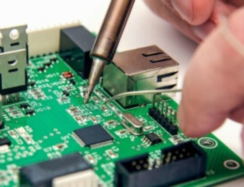
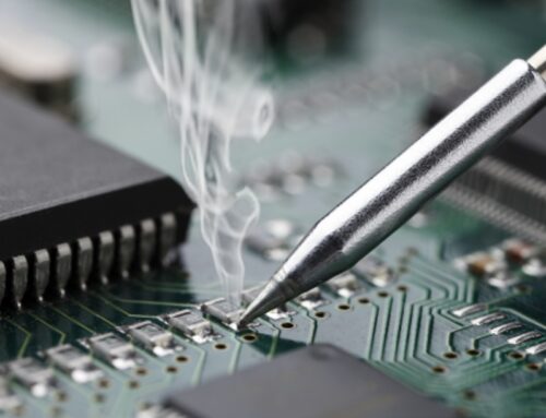
3. Cleaning and Tinning the Welding Iron Tip
If the welding iron is not maintained properly, it will directly affect the quality of hand-welding. The
thermal conductivity of the tip is reduced by contaminants and oxidation. This affects the quality. It
is therefore important to pay close attention to the welding technique. Always clean the tip before
welding with a cleaning cloth. The tip can be repaired if it is severely oxidized with a special
activater. Dip the tip in the activator, and then gently move the tip to allow the abrasive abrasive
work on the surface of the tip until it is shiny again.
The tip should be tinned after completing all the steps above. The tip is covered with a layer to
improve thermal efficiency and prevent oxidation. After welding two or three joints, it is recommended
that you clean the tip again. This will extend the life span of the iron and improve quality of the
joint.
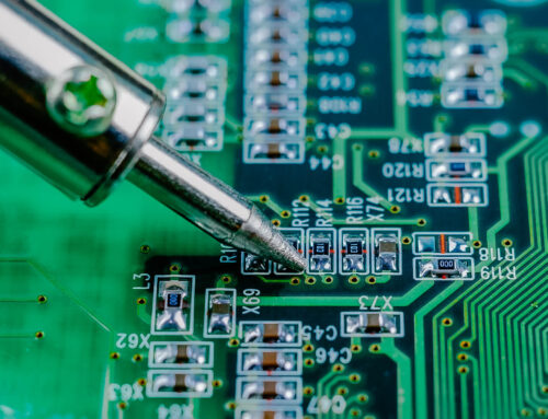
4.Practice Makes Perfect
Practice will improve your welding skills. You can practice your welding skills on practice boards or
scrap circuit boards before you start working with precious and delicate projects. Find the welding
technique that suits your habits and determine the best time for combining welding and iron tips.
Continue to practice and learn to correct mistakes.
Micro-welding irons that look like pens have been introduced to the market in order to improve
convenience. This type of welding tool integrates temperature control and display circuits in the handle
to make the process smoother.
5. Cooperate with an Experienced Printed Circuit Board Assembly Company
You will make a good decision if you consider manual welding, self-sourcing, and micro components to be
too difficult. This will help you avoid a lot of problems during the PCB assembling process.
related Posts
Contact us
WhatsApp: +86-13570802455
Wechat: +86-13570802455
Teams: alek_youte
Email: sales@yt-electronic.com

