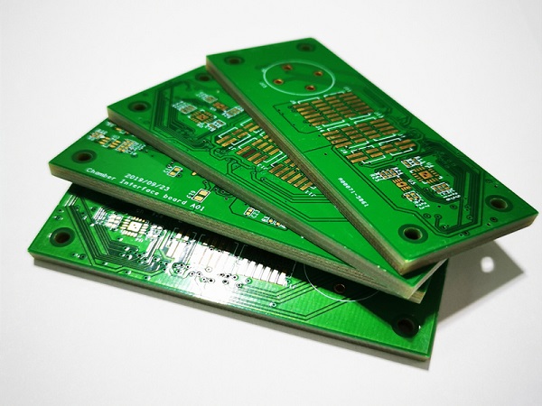
Laying out a multilayer PCB will be similar to making a six-layer, simple cake. It will require more skill and time to make the cake, but it will also be a happy design challenge. In our multi-layer design tutorial, we will show you some of the new methods that will be required to design your PCB.
Step 1 of the Multilayer PCB Design Tutorial: Preparation and Setup
You may need to add layers or attributes to the schematic if an older PCB is not large enough. You can add layers to your schematic depending on the CAD software you use. This is where access to an advanced PCB design software with links to online libraries can be very useful. PCB prototyping is easier when you use the most recent and accurate PCB package data.
The layer stacking is the main difference between a two-layer and a multi-layer board.
When planning your board stack, here are some important points to keep in mind:
Performance: Circuit running speed and final working environment can influence the materials used for circuit boards. You may find that a higher-grade material than FR-4 is more appropriate for your requirements. These materials can still affect certain parameters, such as the impedance calculation. PCB manufacturers can be a great source of information.
Cost: The cost of a circuit board is directly affected by the manufacturing materials, PCB layers and configuration. Your manufacturer should discuss all your options.
Density: The routing densities of the board are another factor that determines the PCB stack-up configuration. After you've started your layout, it can be very difficult to add more layers to the board design. You may have to change the CAD database and make changes to the board layout. If you begin with too many layers you will end up paying more for the board.
Circuit: It is important to know the requirements of the circuit in order to create the optimal layer configuration. For example, for sensitive signals, a stripline configuration may be required to achieve the best performance. This would require adding more circuit board groundplanes. Separating analog and digital circuits will require the use of ground planes. The board power supply will also need to remain isolated. This can have an impact on the layer configuration. Therefore, it is important to plan this before you begin the layout.
After the data is collected, and the board layers stack has been created within the layout database you can start placing and routing the boards.
The Board Outline Generator allows you to create an easy board layer stack.
Views From Different Locations and Routes
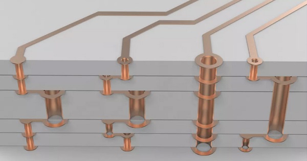
One of the most important things to consider when working on a multilayered layout is the 3D aspects. In a two-layer board, you only need to think about the top and bottom. Now, you're in a world of multiple layers with a lot going on. These can be on the top or bottom. You may not want to put a noisy component in a particular location due to sensitive routing below.
The tools used to place components on the board will be identical, but their appearance will differ. You won't need to leave enough space between the parts you want to route, for example, because they will be routed on internal layers. For sensitive circuits, you'll need to use short and direct paths. In most cases, however, you will have more room to work. This is also a good thing because a multilayer board may require you to place more components.
Here are some important considerations to make in the interim:
Multilayer boards have a greater number of components and routing than dual-sided boards. Plan ahead. Some circuit boards may require specific widths, spaces, or other requirements.
Certain routings will require a structure of stripline layers and must be done on a layer close to the ground plane. To reduce the possibility of broadside coupling and crosstalk, sensitive routing should also cross adjacent internal signal layers vertically.
The ground plane has many holes for connections. However, these vias can affect the return path of the signal. You must plan your routes carefully to avoid blocking the signals.
Arrange the split planes in a way that sensitive signals don't cross over the split and disrupt their return path. This would create a lot noise on the board.
After you have verified the layout and routing of the board, the rest will function like a double-sided design. You are now ready to construct the board.
Circuit board design requires a 3-D perspective when designing multi-layer PCBs.

Finish Your Design By Completing It with Output Files and Documentation
Yt-electronic Printed Circuit Board Assembly Services: In order to put a multilayer PCB into production, it is necessary to create the same documentation as you have always done, with some exceptions. You will first need to add more details to your manufacturing drawings. You will need to include stackup information for your multilayer board in your manufacturing drawings, along with instructions on how to construct this board. If you use Gerber files to manufacture your boards, you will need to create additional files.
Fortunately PCB design software already has the tools necessary to design multi-layer boards. The CAD PCB designer is a powerful system that includes an online CAD service, a wizard for creating board outlines, as well as tools to generate manufacturing and documentation.


