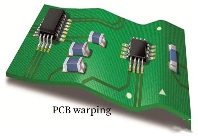
Bending and Warping Are Two Common Deformations of PCBs during the Reflowing Process.
Bending: The Board is bent in whole or part. This can be due to uneven mechanical or thermal stresses.
Warping: The PCB appears bent or twisted on the circuit board. This is due to the thermal stress that occurs during PCB assembly.
Here Are the Main Causes of PCB Warping and Bending:
The PCB board may deform during the reflowing process due to thermal stress generated by temperature fluctuations.
• The PCB board's material properties also influence its deformation potential. Materials with a high thermal expansion coefficient, for example, are more likely than others to deform.
• The PCB design also influences the likelihood of deformation. The larger and heavier the PCB, for example, the greater the likelihood of deformation.
Follow These Steps to Prevent PCB Boards from Warping and Bending:
• Temperature Control: It is important to control the temperature of the reflow-oven accurately in order to prevent deformation due thermal stress.
Avoid abrupt temperature changes and use a reflow-oven with a lower temperature gradient to reduce thermal stress.
• Preheating Stage: The temperature of the PCBs is increased gradually during the preheating phase. It reduces the thermal stress.
• Control of cooling stage: Controlling the speed at which the cooling stage is carried out to prevent excessive cooling that causes thermal shrinkage and board warping. The use of progressive cooling can reduce thermal stress.
• Hot Board Design: We can adjust the shape and distribution of materials on the PCB to make the board more stable in the reflow process.
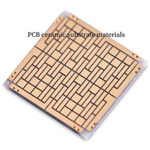
• Material Selection: Select materials with a low thermal expansion coefficient in order to reduce thermal stress. Material with a high degree of rigidity will also help reduce the chance of the PCB board bending or warping.

• Process Optimization: Use a low temperature lamination process during the manufacturing process. Also, use uniform heating reflow and low force drilling processes to reduce mechanical and thermal stresses.
• Deformation detection: Do a denaturation detector after completing PCB board manufacture. This can detect any issues that could cause warping and bending.
The comprehensive improvements above can prevent PCB boards from warping and bending during the reflow process. This will ensure the production of stable and high-quality electronic products.


