Why Is Silkscreen Printing Important for PCB Assembly and PCBA Processing?
This article explains how important screen printing is for PCBA processing and assembly.

You may have wondered how surface mount SMT machines can precisely place electronic components on
printed circuit boards with tight tolerances.
SMT vision systems have many goals: locating the exact position on the circuit for a
component, determining the PCB’s position in the x-y-z plane, and matching the circuit patterns of
the artwork with the printed circuit boards and . The PCB can be positioned using an indexing system.
However, this positioning isn’t precise enough to place components. Silkscreens provide reference
points for imaging systems.
What Is Silkscreen?

The term “fiducial”, although it may sound like a financial word, refers to an object or
surface that is used as a reference or directional measurement for imaging and indexing systems.
Silkscreens can be used for a variety of industries and applications, including physics, computer
graphics in 3D, optics and photography. Silkscreens are used to measure geophysically, to locate the
location of a game board or composite image in augmented reality, and to correlate body scans to body
positions in medical imaging.
Silkscreens are used as alignment marks in automated electronic assembly to align PCBs correctly and in
the right direction. Screen-printing systems allow for precise insertion of circuit components.
Silkscreens are also called “circuit pattern identification marks” and they play a crucial
role in the automated manufacturing process, from testing to packaging.
It is important to not underestimate the importance of silkscreen placement. If at any stage of the
assembly process the exact location of a board or circuit cannot be measured accurately, an automation
“train wreck” will occur!
How Does the Placement of Silkscreen Affect Component Insertion?
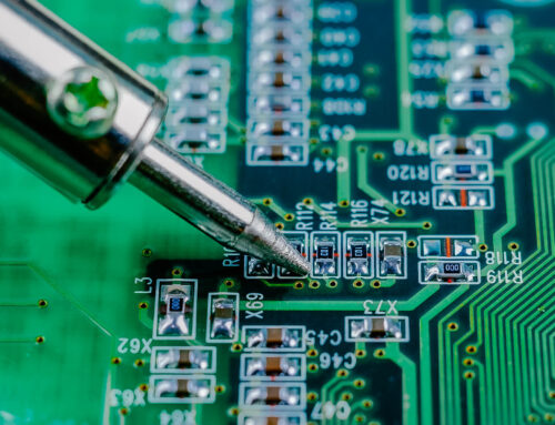
A precise silkscreen placement will ensure that your PCBs are oriented correctly and as perfectly
aligned as possible. SMT placement machines employ cameras to find the silkscreen, and then adjust
component position based on exact board location.

The disadvantage of robotic assembly arms are that they don’t tell you how long they worked.
A conveyor belt is used to feed PCBs into SMT machines. The PCBs are held in slightly different
orientations. This slight difference can ruin the board, unless the calibration is done. Two or three
fiducials on the PCB are marked to help the robot determine the orientation.
The vision system calculates the “offset”, or the distance to which the part should be moved,
by comparing its actual position to the board layout stored in the memory of the machine.
How Do You Set the Silkscreen on a Printed Circuit Board
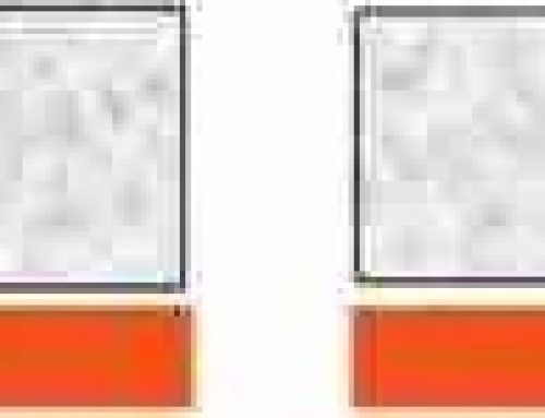
A solder mask is used to leave a circular part of the printed circuit boards uncovered. In this circular
area the copper plating is visible. To ensure good image recognition, the background of the silkscreen
must be “matte”. The fiducials may also be covered by a solder mask as the vision system will
still detect the copper circles.
The machine can identify the location of the PCB by its X, Y and tilt in the clamp using the first two
fiducials. A third fiducial is used to compensate for shrinkage and stretching of the PCB.
Fiducials are required on both sides of a PCB if components are to be placed there. The multiple
silkscreen placements used for PCB positioning is called “global Fiducials”. Components that
require high precision can have a “local fiducial”, which is placed close to the component.
What Happens If You Don’t Use Silkscreen?
Silkscreening is not necessary if you are manually assembling prototypes or single boards. If you are
planning to automate production, you may need to use SMT placement machines, which require reference
points to align the PCBs. Manual assembly also results in boards that fail to meet quality and testing
standards. This means a greater percentage of boards will not pass.
Silkscreen Placement Tips
Here’s some advice on how to place silkscreen on printed circuit boards:
1. A silkscreen’s optimal size should be between 3 mm and 1 mm. You should aim for
a “buffer” matte area that is approximately the same size as your mark’s diameter.
2. Silkscreens must not contain solder masks, unless they are transparent.
3. Global fiducials should have at least two marks and preferably three to ensure
accuracy of component placement. The marks should be placed at the opposite ends and as far away as
possible from each other on the board. Place 3 silkscreens in a triangular pattern and as far apart as
you can on the board.
4. A global silkscreen may be necessary if there is insufficient space on the
board’s edge.
5. The distance between the silkscreen and the edge of the board, excluding the buffer
zone around the silkscreen, should be 0.3 inch.
6. Place at least two silkscreens on the outer edges of a component, diagonally.
Silkscreens locally can be used to correct any placement errors.
7. Where silkscreens are placed can be the difference between an assembly line that
runs smoothly and one which requires constant adjustments. It is still advisable to incorporate
silkscreens in your printed circuit boards, even if the supplier claims that their machine has been
upgraded to function without marks. These marks may be needed if rework is required in the future.