Shenzhen SMT Patch Processing Technology
Yt-electronic has 6 years of SMT processing experience in Shenzhen, with high product quality and fast delivery.


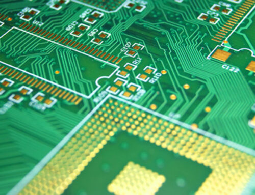
The electronic assembly industry uses SMT as the most common processing technology. This processing
technology can reduce costs and increase production efficiency. This processing technology is used in
the processing facility of yt-electronic. SMT is divided into two types of patch processing:single-sided and dual-sided. It can also be broken down into mixed
assembly and assembly. Today I’ll show you how.
Single-Sided Assembly:
Inspection of incoming material – Screen printing solder glue (apply SMD adhesive) – SMD – Drying
(curing), reflow soldering, cleaning and inspection
Double-Sided Assembly:
A: Inspection of incoming material – Screen Printing Solder Paste (Apply SMD Glue) on
the PCB A Side – Screen Printing Solder paste (Apply SMD Glue) on the PCB B Side – SMD – Drying – Reflow
soldering.
B: Inspection of incoming material – Screen printing solder paste on PCB A-side – SMD –
Drying (curing), Reflow soldering A-side – Cleaning, Flip board – Applying SMD glue to PCB B-side SMD
Curing Wave soldering B-side Cleaning, Inspection and Rework.
This technology can be used for wave soldering and reflow on the A side of the PCB. This processing
technology can be used for SMDs that are assembled on the PCB’s B side with only SOT or SoIC (28
pins) or less.
Mixed Assembly with Single-Sided:
Incoming material inspection (screen printing solder paste) – SMD (drying/curing) – Reflow soldering
(cleaning) – Insertion (wave soldering) – Cleaning & Inspection Rework
Double-sided mixed assembly
A: Inspection of incoming material – Applying SMD glue to PCB B Side – SMD – Curing –
Flip board Insertion onto PCB A Side Wave soldering on PCB A Side Cleaning — Inspection — Rework
If there are more discrete components than SMD components, it is best to apply first and insert
afterwards
B: Inspection of incoming material – PCB A surface plug-in (pin-bending) – flip board
PCB B Surface SMD glue SMD – curing – flip board Wave soldering cleaning inspection rework
If there are more discrete parts than SMD, it is best to plug in first before sticking.
C: Inspection of incoming material – PCB A surface solder paste screen printing – SMD –
drying – reflow soldering, pin bending, flip board, PCB B Surface SMD glue, SMD, curing, flip board,
wave soldering, cleaning, inspection, rework, A surface mixed.
D: Inspection of incoming material – PCB A Surface screen printing solder paste, SMD –
A surface reflow-soldering – plugin – B surface wave-soldering cleaning inspection rework A and B
surface mounting. Initially, paste the SMD on both surfaces, then reflow soldering. Then insert and wave
sell.
E: Incoming Material Inspection => PCB A side mounting and B side mixed assembly.
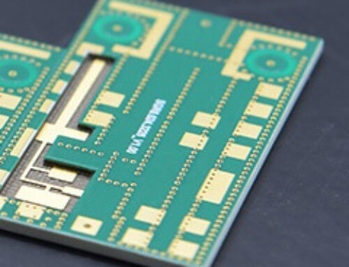
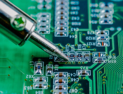
You can see the above picture of Shenzhen SMT’s single-sided and dual-sided patch processing.
Yt-electronic is available for consultation at any time. Yt-electronic is a Shenzhen-based SMT
manufacturer with 6 years’ experience. We offer high quality products and quick delivery.
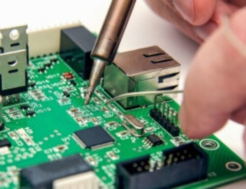
Shenzhen PCB assembly is a well-established electronic processing facility in Shenzhen that can offer SMT
processing. The company has a wealth of experience in PCBA assembly. PCBA can be your one-stop shop.
Yt-electronic also offers DIP plug-in production, PCB manufacturing, and electronic circuit boards.