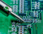
Application of AOI to SMT Manufacturing
This article mainly describes the application of AOI technology in SMT manufacturing, from printing, mounting, welding, etc.


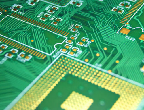
AOI is a technology that can be used to inspect all components, including welding and mounting, in SMT
manufacturing.
Main Applications of AOI
The AOI is used primarily in component inspection, solder paste printing inspection and after-welding
inspection.
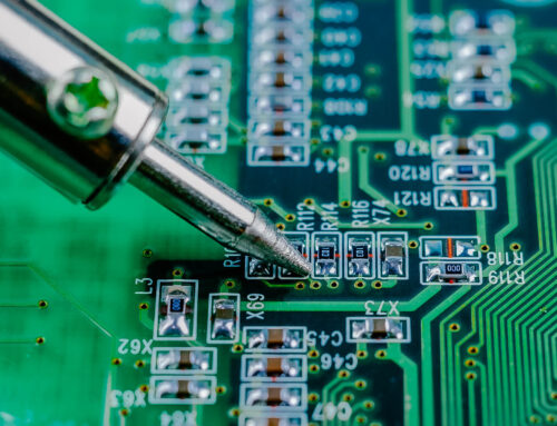
1. Stencil Printing
AOI is a key component of the SMT print process. AOI can be used to detect and verify that the solder
paste is in the correct position, uniformity and quality.
AOI’s high-resolution imaging can identify excessive or insufficient solder to ensure the proper
distribution of the PCB.
2. Component Placement
AOI can be used during the placement process to ensure that all components have been placed correctly.
It can determine the component’s orientation, position, and polarity in order to verify that it
meets the design drawings.
AOI can also detect potential errors in printed circuit board assembly, such as components that are
tilted or offset, and missing components to avoid these issues leading to more serious quality problems.

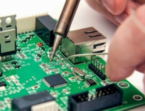
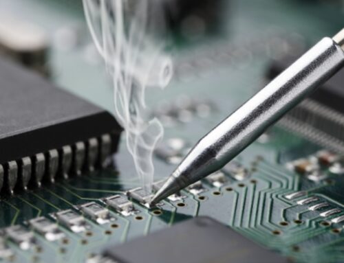
3. Reflow Soldering
During welding, the AOI System inspects solder joints for quality and connectivity. It can detect if the
solder joints insufficient or excessive and if there are any problems such as cold joints,
short-circuits or open circuits.

AOI’s real-time analysis of images can identify welds that are not qualified and alert operators to
repair PCBs to ensure final welding quality.
4. After-Solder Inspection
AOI is still used in the post-welding process. It can detect problems with solder joints and components.
The AOI system can help to identify potential quality issues and ensure that the product meets required
standards of quality before moving on to the next stage of circuit card production.
5. Final Inspection
AOI is also used to perform a comprehensive final inspection at the SMT terminal detection stage.
The circuit card is checked for component placement, solder joints, component alignment, and
orientation.
Terminal inspection is the final check to make sure that the PCBs are designed according to the
specifications. AOI achieves the goal of efficient automated inspection.
The Advantages and Challenges of AOI
The application of AOI to SMT processes has many benefits, including:
Increase inspection efficiency: AOI detects defects automatically and efficiently,
saving time on manual inspection.
Increase detection accuracy: The AOI uses image recognition technology to accurately
detect subtle defects.
Reduce production cost: By using AOI, you can reduce your PCB manufacturing costs and
the rate of PCB rework.
There are also some challenges that AOI faces, such as:
High investment costs: The introduction of an AOI requires an initial investment, and
then maintenance. This increases the cost to circuit board manufacturers.
Cannot replace manual inspection: Although automated optical inspection systems can
efficiently detect many problems,It still can’t replace manual inspections, particularly when it
comes to complex defects.
PCB manufacturers should consider these advantages to improve the quality of SMT production.