Printed Circuit Board Assembly(PCBA) Process
This article will introduce the entire process of printed circuit board assembly(PCBA).

A printed circuit board is used in electronic
products like mobile phones, TVS and even cars. How do you put together so many parts to make a circuit
board? This article will explain the whole process of PCBA (printed
circuit board assembly).
PCBA Process Flow
The Printed Circuit Board Assembly Process refers to specific operating steps and requirements for PCB
Assembly. It includes PCB design, fabrication, material procurement and SMT patching, as well as testing
and three-proof painting.
Step 1: PCB Design and Fabrication
PCB design depends on PCB engineers, including PCB schematics and circuit diagrams. After checking, you
can arrange for a PCB manufacturer to produce prototypes and mass production.
Step 2: Design a BOM Table and Purchase Materials
BOM is a detailed material selection and design document that engineers use. It is a detailed document
that defines the product’s structure, based on the PCB drawings of the product and its functions.
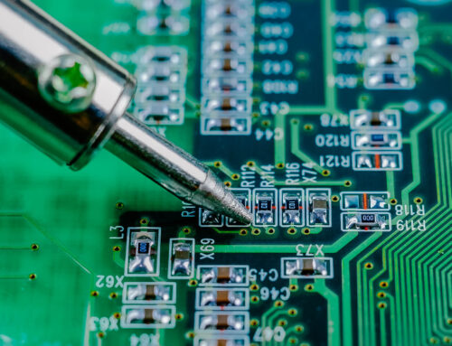
Step 3: Apply the SMT Patch
SMT patches are an important part of PCB assembly, which welds components to PCB substrates. Wave crest
soldering is one of the welding methods. Re-flow soldering and manual welding are also available. Manual
welding with rework is available, as well as wave soldering and reflow welding. After welding, the PCBs
must be cleaned sweep after welding. They will then be dried before being sent to be tested for quality.
1) Solder Paste Is Applied:
Apply the solder paste evenly and correctly to the solder pads on the surface.
Solder paste is composed of tiny metal balls that are composed of 96.5% of tin, 3.5% of silver and 0.5%
of copper. Solder paste is made up of flux and solder. Flux is the chemical that makes the solder stick
and melt.
2) SPI Detection:
It is important to inspect the solder paste after it has been printed using a SPI machine. Checking is
done to verify the quality of the printed solder paste, as well as if there are any tin-leakage or
tin-less problems.
3) Patch:
The robot will then place the surface-mount components on the PCB after applying the solder paste.
4) Re-Flow Welding:
Due to the fact that the soldering paste has no solidifying effects, the component will not be very
solid after mounting. Re-flow welding must then be performed to make the component solid. It is commonly
referred to as melting and cooling at high temperatures. The components are firmly on the board.
Step 4: Insert the Through-Hole Element
The welding method chosen depends on the type and size of the circuit board. There are also PHT or
electroplated through-hole parts. Electroplated through-hole components are holes in the circuit board.
These holes transmit the signal from one side to the other of the board. Solder paste printing through
the holes has no attachment point. This requires a specific soldering technique.
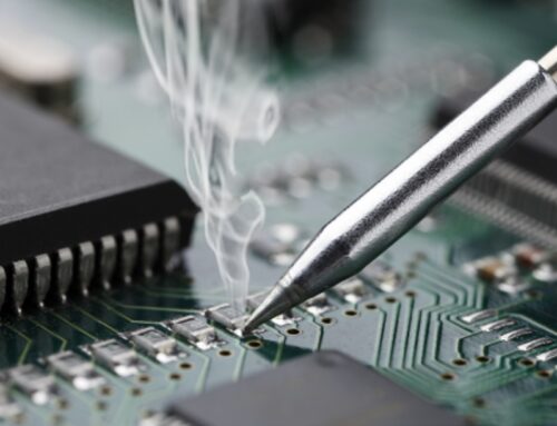
1) Manual Welding:
Manual perforation welding is a good option.
2) Crest Welding:
Then, the conveyor belt is used to send the board directly to the wave soldering machine, which melts
the paste and forms the solder joints. It is then sent via conveyor belt to the wave-soldering machine
to melt the paste and form the solder joints. The components are securely attached to the board.
Step 5: PCB Cleaning
The printed circuit board must be cleaned after assembly to remove any welding traces and contaminants.
The circuit board is cleaned with deionized or improvement solution, then deionized and high-pressure
water is used. Use a powerjet to dry the board after cleaning and send it off for final product testing.
Step 6: PCBA Test
The printed circuit board assembly test ensures the product is working correctly. Some automated tests
detect the PCB and further enhance PCB efficiency and quality. This test includes burn-in, functional,
and reliability tests. The PCBA test is the final and most important step of the process. It determines
whether the previous steps were successful. There are different detection methods.
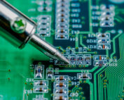
1) Visual Inspection:
We can opt visual inspection for a few boards. The designer can check the PCB and make sure it is of
high quality.
2) Automatic Optical Inspection
This method is ideal for PCBA inspection on a large scale. Automatic optical inspection machines use
high-performance cameras that can detect and observe welding problems from different angles.
3) X-Ray:
Check the inner layer of the printed circuit assembly using infrared.
4) In-Circuit Test System(ICT):
The tester will show the user which component has a fault or where the short is located.
5) QC Manual Inspection:
The IPC-610 standard inspection standard requires that the board be checked to ensure 99.98% quality.
6) QA Inspection of Shipments:
Scanning codes and strict inspections before shipment of products are required to ensure that only
qualified products are shipped.
Step 7: Apply 3 Anti-Paint
By applying conformal coating to the PCBA’s surface, you can protect the PCBA from moisture and
corrosion. This will extend the life of the product. You can now pack and ship your product after
completing the two steps above.
Summary
Is an arduous and complex process. The process must be done step-by-step. Each link is important. Each
link is crucial.