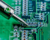
High-Speed PCB Design
This article introduces the advantages and applications of high-speed PCB and the factors that need to be considered in high-speed PCB design.

What Is High-Speed PCB Design
The term High-Speed PCB Design refers to the design of high-speed signals for a printed circuit board (PCB).
The rise and fall time of high-speed signals is typically less than one nanosecond.
This course requires knowledge of electromagnetic compatibility, signal integrity, stacking, wiring
rules and other related topics.
High-speed PCBs are designed to guarantee the reliability and quality of high-speed signals, while
avoiding problems like signal distortion, interference and reflection.
High-Speed PCB Design Considerations
1) Impedance Matching
During transmission, high-speed signals generate electromagnetic fields.
Signal reflections can occur if the signal is not matched to the impedance on the transmission line.
This can reduce the completeness of the signal.
2) Spacing
Other signals, power lines, groundlines, etc., will interfere with the transmission of high-speed
signal. Interference can be reduced by increasing the distance between signals.
3) Length Match
Both lines in the differential signal must be the same length. The signal integrity will be reduced if
the lengths of the two lines are different.
To ensure the integrity of signals in high-speed design, specialized tools and methods are required.
Designers can use specialized tools to analyze signal transmission paths in order to identify problems.
Benefits of High Speed PCB Design
1) Optimize Signal Transmission Performance
The design of high-speed PCBs can improve signal transmission performance. This results in less signal
loss and interference at higher frequencies, thus improving system reliability.
2) Signal Integrity
By using a precise layer stack and layout, you can avoid signal reflection, clock jitter and crosstalk.
3) Power Optimization
By optimizing the circuit layout and layer-stack design, high-speed PCB designs can reduce power losses
and improve system efficiency. This is particularly important for mobile devices and batteries-powered
systems.
4) Improved Heat Dissipation
A high-speed PCB layout that is precise can help improve heat dissipation for high-power devices and
maintain the stability of electronic parts under high-load conditions.
5) Shortened Design Cycle
The use of advanced design tools, simulation technology, and other technologies can speed up the design
process and reduce the time it takes to develop a product. This will improve the market’s
competitiveness.
High-Speed PCBs Are Used in Many Applications
Here are some examples of specific applications:
1) Digital Signal Processing
Digital signal processing (DSP), also known as digital signal processing, is a technology that processes
digital signals.
DSP technology is used widely in electronic products such as audio, video, image, and communication
processing.
DSP systems often need to transmit signals at high speeds, so a high-speed PCB is essential.
High-speed PCBs transmit audio and visual signals in audio and video processing.
2) Communication
Communication systems, like Ethernet, fiber-optic communication, wireless communications, and others,
need to transmit signals at high speeds.
In order to maintain signal integrity and reliability, it is important that communication systems use
high-speed PCB designs.
3) Storage
Solid-state drives, memory and flash storage are all common examples of storage systems.
In an SSD for example, data signals are transmitted using a PCB with high speed.
Data signals are transmitted using high-speed PCBs in memory.
Flash memory uses high-speed PCB to transmit data.
4) Image Processing
Digital cameras, scanners and displays are examples.
Image processing systems require high-speed signals to be transmitted, so PCBs with high-speed design
are essential.
In digital cameras, for example, image signals are transmitted using high-speed PCBs.
High-speed PCBs transmit images in scanners and displays.
Summary
The design of high-speed PCBs is a complex process that requires expert knowledge.
You can make sure that PCBs with high speed can transmit signals effectively and meet system
requirements by ensuring proper design and implementation.